Adding 11KB of RAM to a CP/M 3 system with a single NAND gate chip
Wednesday, 30th August 2023
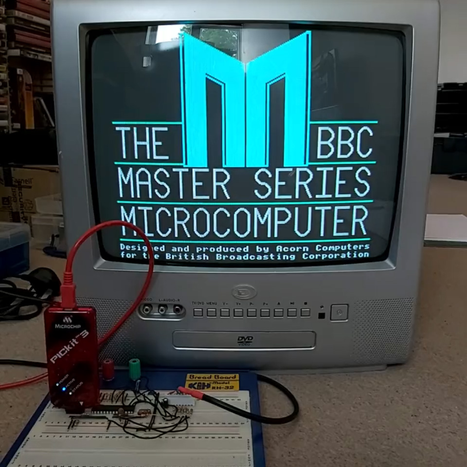
It's been quite a while since I posted about my Z80 Computer project. This is a home-made Z80 computer I built back in 2010 that features a 10MHz Z80 CPU with 64KB RAM that runs CP/M 3. It can drive an internal LCD, TV or VGA monitor at 320x240 (monochrome only) and unfortunately is a project I was never too happy with due to several compromises I had to make in its design – though at the time I was happy enough I got it to work at all! The video output was limited by both my choice to use an internal graphical LCD and the limitations of the dsPIC33F I chose to use to drive it and the software was all a bit half-baked. I could run the generic CP/M version of BBC BASIC on it, but this lacks graphics and sound support, for example.
More recently my work on adapting BBC BASIC to the Sega Master System had reignited my interest in 8-bit programming, though that too was imperfect due to the limitations of the Master System's VDP. I was further encouraged by coming third in the "Retro not Vintage" competition on /r/retrobattlestations, though I'm not sure I was quite worthy of a podium finish.
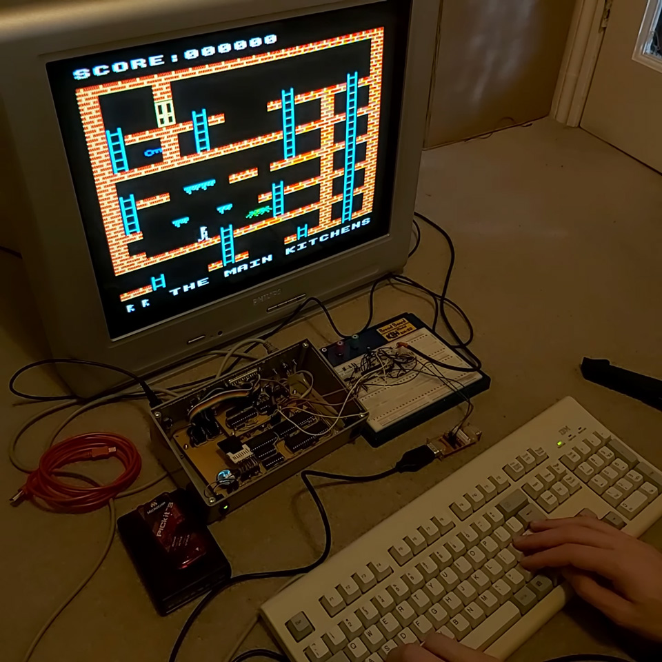
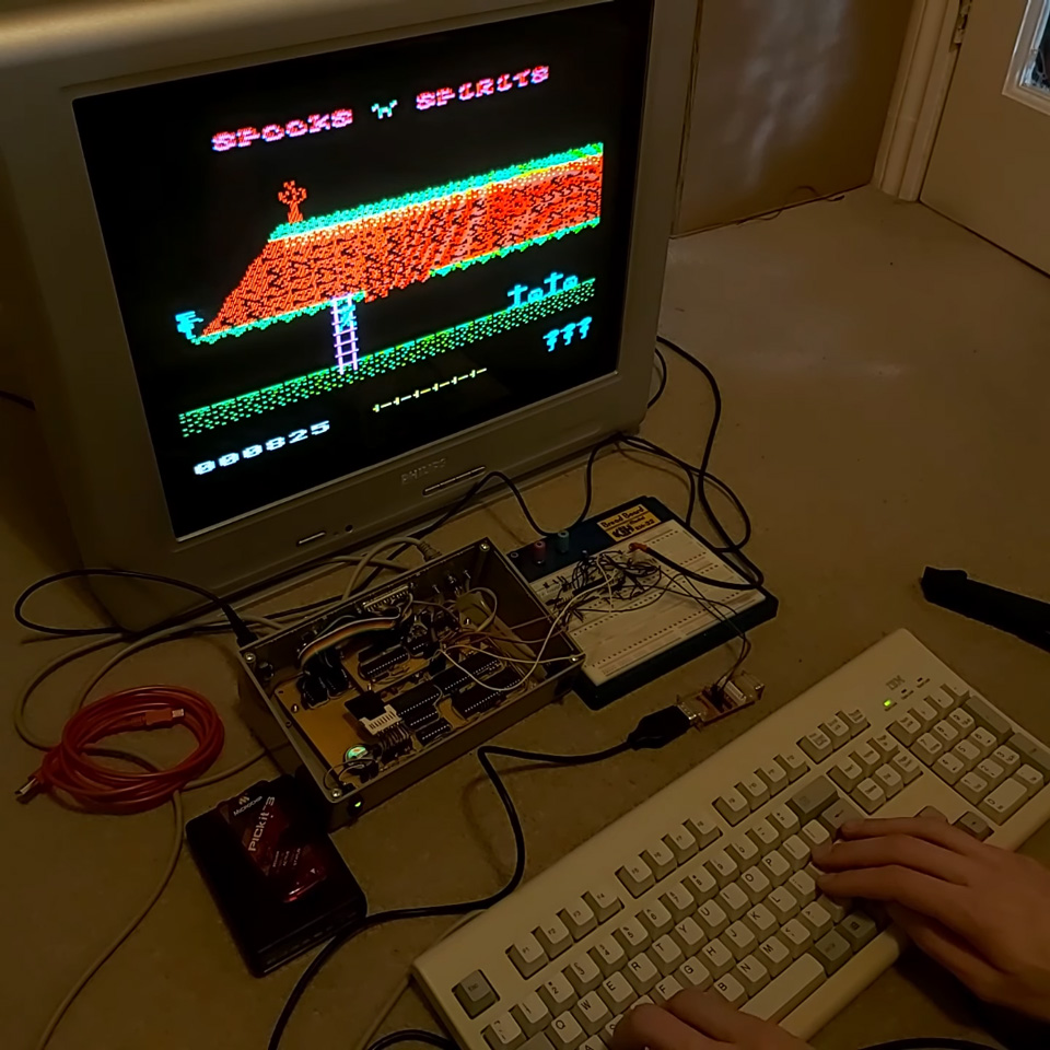
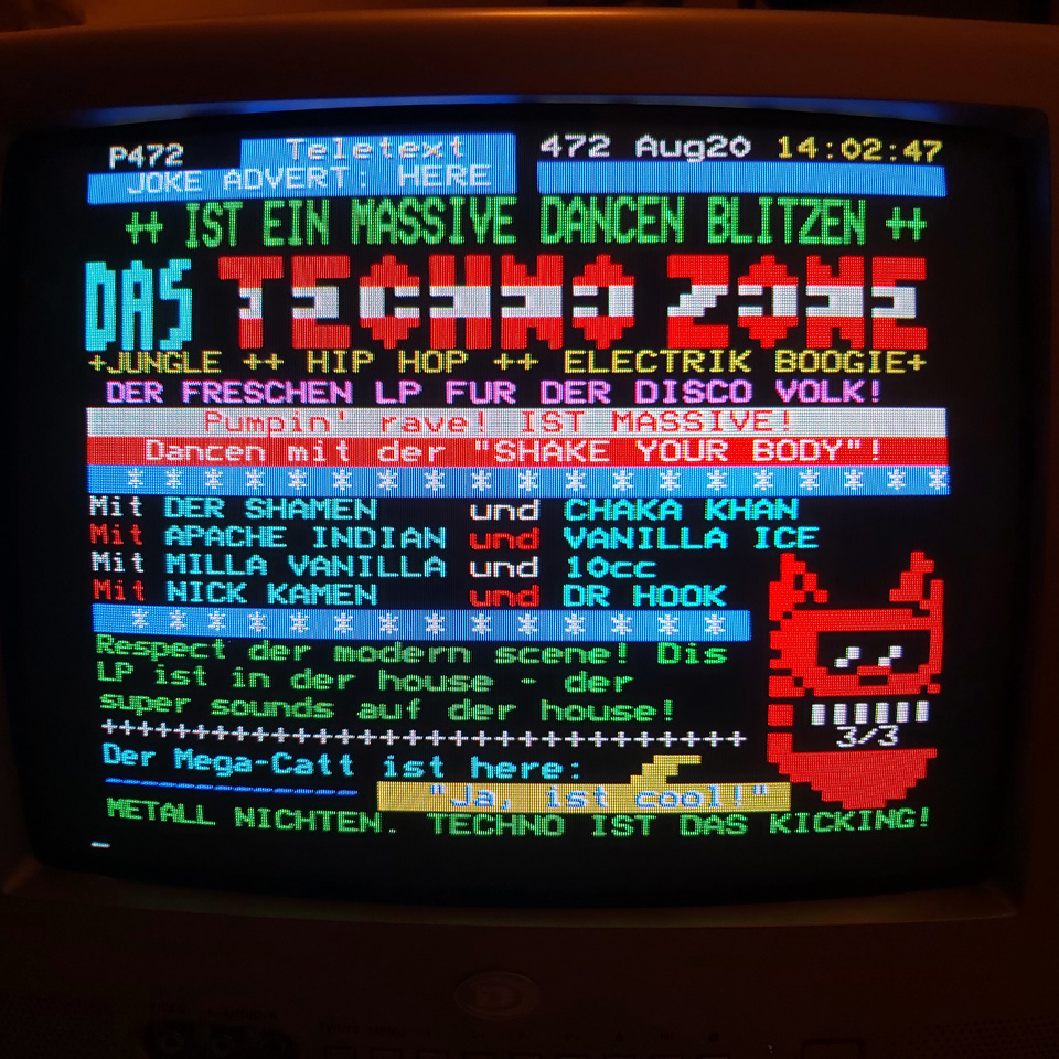
With this in mind I started work on improving the computer. I replaced the existing dsPIC33F VDP with a new one based around a dsPIC33E. This newer microcontroller has 32KB of RAM and can run at up to 70 MIPS, a big upgrade from the previous 16KB RAM and 40 MIPS. This provides me with enough video RAM to store the largest BBC Micro screen mode frame buffer (20KB) as well as the necessary CPU grunt to look up pixel data from colour palettes and output it to the screen. I've implemented all eight of the standard BBC Micro screen modes, from the high-res 640x256 (in two colours) MODE 0 to the low-res 160x256 (in sixteen colours) MODE 2 along with the Teletext-compatible MODE 7. This is all controlled via a BBC Micro-compatible VDU driver and the results all seem quite faithful with no real compromises.
There was even enough CPU power left over on the microcontroller to implement BBC Micro-compatible SOUND and ENVELOPE, and with the source code for the CP/M version of BBC BASIC having been released since I last worked on the project it made it much easier to add all of the graphics and sound routines into the version of BBC BASIC specific to my computer.
To get an idea of what the computer is like to use, I recorded a little demo video here. However, this is not really what I wanted to write about in this post – I wanted to cover an easy way to free up some RAM by implementing banked CP/M 3.
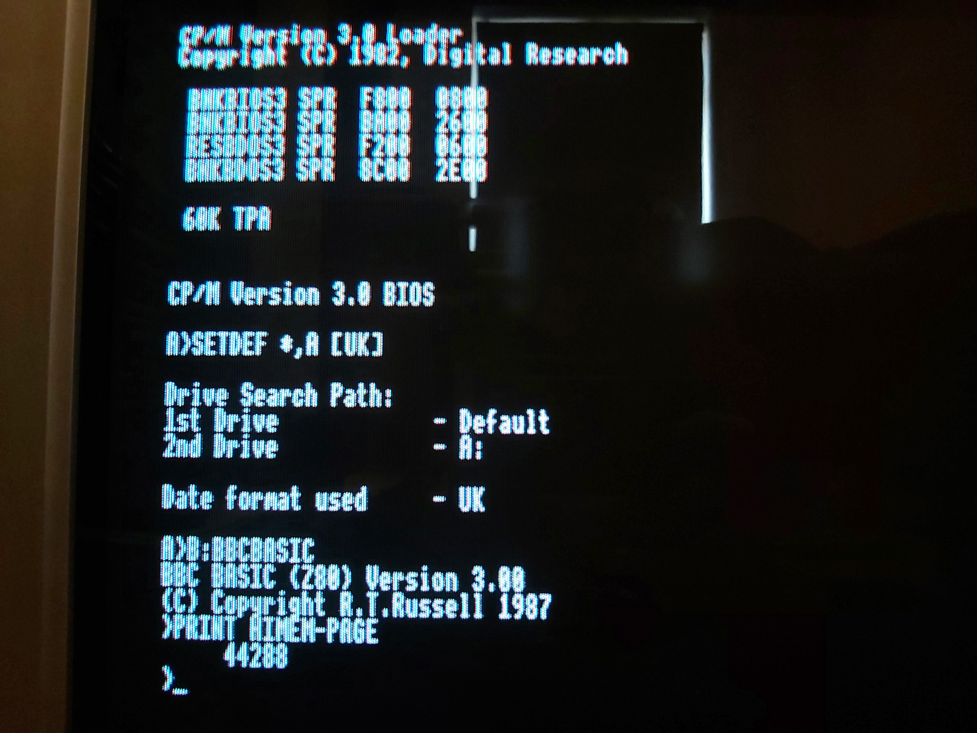
Non-banked versus banked CP/M
I chose CP/M 3 as the OS for my computer instead of CP/M 2 as I'm using an SD card for storage and CP/M 3 has native support for disk sector sizes that do not directly match the file record size and it will handle the blocking/unblocking for you (CP/M's file records are 128 bytes long, SD card sectors are 512 bytes long). One other nice feature of CP/M 3 is the existence of a "banked" version which allows it to run on systems with more than 64KB of RAM. As far as user programs are concerned they still run in a flat 64KB memory space, however the OS can move certain parts of itself as well as disk and directory buffers into a separate memory bank where they are only accessed when needed, freeing up space in the "transient program area" (TPA). As well as more memory for user programs the banked version provides a much improved line editor when typing at the command-line, password protection of files and more descriptive error messages.
Naturally, when I read about this I thought it would be an obvious choice for my computer. As it is, I'm using a 128KB RAM chip but have tied A16 low as I didn't have any kind of MMU or bank-switching hardware setup (32KB and 128KB RAM chips are available in abundance, 64KB ones less so, and using a 128KB chip with the address line tied low involved a lot less soldering than two separate 32KB RAM chips). I did have an emulator where I could try to prototype the hardware changes to support a banked CP/M 3, however I was not able to get a banked version of the OS built and working so gave up – after all, I had a 49KB TPA, which seemed like it would be good enough.
With the other improvements to the computer recently I thought it worth reinvestigating. I did a bit of hunting to see if I could find any recommendations for a simple setup but most of what I could find ended up being a lot more complicated than what I was really looking for. After a bit more experimentation I was able to end up with a banked version of CP/M running on my computer and all I needed was a single NAND gate chip.
Memory requirements for banked CP/M
The memory layout of banked CP/M is actually quite a bit simpler than a lot of the threads I could find online seemed to make out. All you really need is a shared common area at the top of memory that will always be accessible regardless of the current state of the selected bank, and memory below that which can be switched between multiple banks. When booting the computer bank 0 will be selected, so both the common (resident) and banked parts can be copied to memory, and then bank 1 will be swapped in to provide the large TPA.
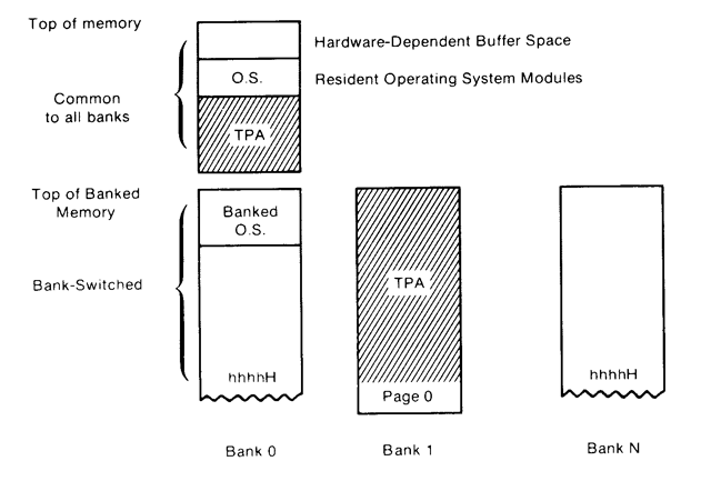
In my case, as I'm using a 128KB RAM chip, I will use A16 as the bank selection bit. When low this will provide access to the lower 64KB RAM on the chip, when high it will provide access to the upper 64KB RAM. To implement the common area at the top of memory, you then just need to check to see if the address is above the boundary between banked and common memory and if so to force A16 either high or low (it doesn't matter which, as long as it's consistent) so that when the address is in the common area the same bank will be accessed, regardless of the state of the bank selection bit.
Bank switching with simple logic
A simple way to implement a common area in upper memory is with AND (to detect the high address) and OR (to force the A16 high if it's a high address) logic, like this:
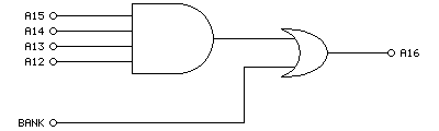
Here we use a 4-input AND gate to detect any memory address in the top 4KB of the chip (address lines A12 to A15 will go high at %1111000000000000 which gives a common region of $F000 to $FFFF). If that's the case, then the output of the 4-input AND gate will be high, which when ORed with the bank selection bit will force A16 high whenever we're in the common memory area. If we're below the common memory area then the value of the bank selection bit will pass through directly to A16, allowing us to bank switch the lower area of memory. Or, to summarise in a truth table:
| In | Out | ||||
|---|---|---|---|---|---|
| A12 | A13 | A14 | A15 | BANK | A16 |
| 1 | 1 | 1 | 1 | x | 1 |
| 0 | x | x | x | 0 | 0 |
| 0 | x | x | x | 1 | 1 |
| x | 0 | x | x | 0 | 0 |
| x | 0 | x | x | 1 | 1 |
| x | x | 0 | x | 0 | 0 |
| x | x | 0 | x | 1 | 1 |
| x | x | x | 0 | 0 | 0 |
| x | x | x | 0 | 1 | 1 |
However, it would be easier if we could implement this on a single chip. A 4x 2-input NAND gate chip (such as the SN74ALS00AN) should do the job when wired up as follows:
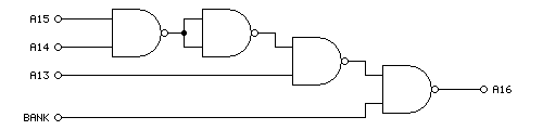
The truth table is a little different this time around:
| In | Out | |||
|---|---|---|---|---|
| A13 | A14 | A15 | BANK | A16 |
| 1 | 1 | 1 | x | 1 |
| 0 | x | x | 0 | 1 |
| 0 | x | x | 1 | 0 |
| x | 0 | x | 0 | 1 |
| x | 0 | x | 1 | 0 |
| x | x | 0 | 0 | 1 |
| x | x | 0 | 1 | 0 |
When accessing the banked region of memory A16 is the inverse of the bank selection bit. This doesn't matter, though, as long as there's a consistent mapping between logical addresses and the physical RAM addresses it will work even if it's "backwards". There's also one fewer address line, which means that the common area now runs from %1110000000000000 = $E000 to $FFFF, providing a common area of 8KB. In practice I didn't find this made a difference to the amount of memory available in the TPA; whether the common area was 4KB, 8KB or 16KB I was able to bring the TPA up to 60KB (from 49KB in the non-banked system), though it does eat into the amount of memory available on page 0 for disk and directory buffers. As I'm loading from an SD card (which is much faster than the floppy discs of yore) the reduced buffer space is less of a concern to me.
Fortunately there was enough space inside the computer (and a single remaining pin on the I/O controller to act thas bank selection bit) to add the NAND chip and drive A16. At last I have access to 120KB of my 128KB RAM chip... but what about the software?
Building a banked version of CP/M
I will start with the assumption that you have been able to build a non-banked version of CP/M 3 and got that running on your computer, as there is a lot less that can go wrong when doing so. Once you've got that working there's not too much to add to your BIOS to make it support banking, however I did run into a few issues with missing files and some misinterpretation of how things should work until I was able to get it working.
I used the "Developers Build Directory for CP/M 3" from The Unofficial CP/M Web site as my source for CP/M 3. This contains the GENCPM tool that will be used to generate the CPM3.SYS that will need to be loaded into memory by your boot loader. In my case I get my I/O controller to copy CP/M from the SD card into memory at boot – if you've already got the non-banked version of CP/M 3 booting then you'll be familiar with this, but do pay attention to table D-1 in the CP/M 3 system guide which points out the two parts of CP/M to load – the "resident" and "banked" portions. Both parts need to be loaded on a banked system, and both need to be loaded into page 0.
To get that far you will need to have relocatable copies of your banked BIOS (BNKBIOS3.SPR) and the BDOS (RESBDOS3.SPR and BNKBDOS3.SPR) ready to be used by GENCPM. I couldn't find a ready-made copy of these BDOS modules, but you can build them using RMAC and LINK as shown below:
RMAC RESBDOS
LINK RESBDOS3=RESBDOS[OS]
PIP BNKBDOS3.ASM=CPMBDOS2.ASM,CONBDOS.ASM,BDOS30.ASM
RMAC BNKBDOS3
LINK BNKBDOS3=BNKBDOS3[OS]
The banked BDOS source code is split between three different source files which need to be combined with PIP first, then can be built. For the sake of completeness, if you wanted to build the non-banked BDOS3.SPR you'd use a very similar set of commands, just with CPMBDOS1.ASM instead of CPMBDOS2.ASM:
PIP BDOS3.ASM=CPMBDOS1.ASM,CONBDOS.ASM,BDOS30.ASM
RMAC BDOS3
LINK BDOS3=BDOS3[OS]
The other important ingredient is your banked BIOS, BNKBIOS3.SPR. I don't get on with 8080 syntax so I assemble my BIOS3.MAC with Microsoft's M80 in Z80 mode (instead of RMAC).
RMAC SCB
RMAC BIOSKRNL
M80 =BIOS3
LINK BNKBIOS3[B]=BIOSKRNL,BIOS3,SCB
If you had previously edited BIOSKRNL.ASM to state banked equ false remember to change it to banked equ true as well!
The only additions you should need in your BIOS are implementations of ?xmove and ?bank. ?bank is an easy one, and just switches to the memory bank requested in the A register. In my case I handle that just by outputting A to the I/O port that handles bank switching:
; Select Memory Bank
; Entry Parameters: A=Memory Bank
; Returned Values:  None
; You must preserve or restore all registers other than the
; accumulator, A, upon exit.
?bank:
if banked
	out (bank$select),a ; change this for what your hardware requires
endif
	ret
(To retain compatibility with my old banked BIOS I wrap the changes in an if banked condition – banked equ true appears earlier in the file).
?xmove is a little more complicated – this states that the subsequent ?move operation (which copies BC bytes from DE to HL) should transfer data from one memory bank to another. Note that this only affects the next ?move operation; if ?move is called again afterwards without ?xmove then it should perform a copy within the same bank as before.
Fortunately the inter-bank copy is limited to 128 bytes so you can simply implement this by temporarily copying the data from one bank into a 128 byte buffer in common memory, then copying the data back to the destination bank. It's not exactly efficient, but it keeps the hardware simple.
; Memory-to-Memory Block Move
; Entry Parameters: HL=Destination address
;                   DE=Source address
;                   BC=Count
; Returned Values:  HL and DE must point to
;                   next bytes following move operation
?move:
	ex de,hl
	ldir
	ex de,hl
	ret

; Set Banks for Following MOVE
; Entry Parameters: B=destination bank
;                   C=source bank
; Returned Values:  None
?xmove:

if banked
	; Store the source/destination bank numbers
	ld (mov$src$b),bc
	; Make sure that the next call to move (via ?mov vector) uses the banked move routine.
	ld bc,banked$move
	ld (?mov+1),bc
	ret

banked$move:

	; Select source bank
	ld a,(mov$src$b)
	call ?bank

	; Swap registers from CP/M to Z80 conventions
	ex de,hl

	; Preserve destination and length
	push de
	push bc

	; Copy from source to buffer
	ld de,mov$buf
	ldir

	; Recover length and destination, preserve source
	pop bc
	pop de
	push hl

	; Select destination bank
	ld a,(mov$dst$b)
	call ?bank

	; Copy from buffer to destination
	ld hl,mov$buf
	ldir

	; Recover source
	pop hl

	; Swap registers from Z80 to CP/M conventions
	ex de,hl

	; Make sure that the next call to move (via ?mov vector) uses the regular move routine.
	ld bc,?move
	ld (?mov+1),bc
	ret

mov$src$b:
	db 0
mov$dst$b:
	db 0

mov$buf:
	ds 128
else
	; Unbanked
	ret
endif
This implementation works by changing the ?mov vector in the BIOSKRNL to point at our banked$move routine after a request to ?xmove. Once we've carried out the banked move, the original ?move routine is restored to the ?mov vector.
Once you have assembled and linked your BNKBIOS3.SPR, RESBDOS3.SPR and BNKBDOS3.SPR you can use GENCPM to create your new CPM3.SYS. You'll need to answer some questions differently to support the banked system:
- Bank switched memory? Y.
- Common memory base page? E0 (if using the NAND gate circuit above – our common area starts at $E000).
- Number of memory segments? 1 – we have three in total (bank 0, bank 1 and common) however bank 1 and common are not included in the segment table so should be ignored here.
- Memory segment table base, size, bank: 01, 90, 00 (we want to keep CP/M out of the "zero page" so start the segment from $0100, CP/M 3 starts at $9100 so we have $9100-$0100=$9000 as our size, the bank number is 0).
Before being prompted for the memory segment table GENCPM will display where CP/M 3 itself is using memory so you can use that to figure out how much free space you have on your bank zero for your segment definition. However, if you enter a value that is too large GENCPM will automatically reduce the size for you.
After this you will be prompted to create disk and directory buffers for each of your disk definitions – pay attention to available space to get an idea of how many buffers you can create, but if in doubt just allocate a single buffer for each disk/directory as prompted as that will at least get you booted, then you can experiment with larger buffers later.
I did intentionally start my segment from $0100 instead of $0000 and this is to avoid problems with interrupts and to keep the zero page free. My computer design uses interrupts to signal to the Z80 that keys are available (for example) instead of requiring it to constantly poll the I/O controller. However, I did find that if I interrupted the CPU (e.g. by pressing a key) when it had switched over to page 0 it would hang the computer as the ISR vector had been switched out from underneath it. My ISR is in common memory and I just make sure that when the computer boots it installs its interrupt vectors in every memory bank so that it doesn't matter which is currently swapped in, it'll always find its way to the common ISR.
After making these changes I was greeted with a 60KB TPA instead of the previous 49KB TPA – 11KB of extra memory is well worth it, and the improved line editor in CP/M 3 is another nice bonus. I did think that implementing this was going to be a nightmare, but in the end I only needed one extra NAND gate and a few easy changes to the software.
Addendum (31st August 2023): One other change you will need to implement is to support disk operations reading from or writing to specific memory banks. I forgot to mention this earlier as it's handled by the setbnk routine inside BIOSKRNL, and that routine stores the selected DMA bank number in the @dbnk variable. When your BIOS performs a disk read or write operation it will need to preserve the current bank number, switch to the bank number in @dbnk, carry out the read or write operation, then restore the previous bank number.
In my case, disk I/O is handled by the AVR I/O controller where operations are set up by sending over the DMA address, sector and track numbers, drive index and then performing a read from either the "read" or "write" ports to initiate the I/O operation and retrieve the status. The only change required was to make sure that the bank number is also sent over before initiating the I/O request so the AVR knows which bank it should be accessing:
fd$copy$ptrs:

	ld hl,(@dma)
	ld a,l
	out (disk$dma$l),a
	ld a,h
	out (disk$dma$h),a

	ld hl,(@sect)
	ld a,l
	out (disk$sector$l),a
	ld a,h
	out (disk$sector$h),a

	ld hl,(@trk)
	ld a,l
	out (disk$track$l),a
	ld a,h
	out (disk$track$h),a

	ld a,(@adrv)
	out (disk$drive),a

	if banked
		ld a,(@dbnk)
		out (disk$dma$bank),a
	endif

	ret

fd$write:
	call fd$copy$ptrs
	in a,(disk$write)
	ret

fd$read:
	call fd$copy$ptrs
	in a,(disk$read)
	ret
I'm pretty sure I didn't forget anything else!