Z80 computer with a primitive I/O board
Wednesday, 20th August 2008
A computer needs some way of interacting with the outside world via input and output devices. It's about time, then, that the Z80 computer project acquires a section dedicated to I/O.
The Z80 differentiates between memory and I/O devices, though both share the data bus and the address bus. You can control I/O devices using the in (input) and out (output) instructions. When you input or output you must specify a device address and a value or target register. For example,
    in a,($20) ; Read a value from device $20 and store it in A.
    ld a,123
    out ($40),a ; Output 123 to device $40.
When you write to a device, the following happens:
- The address bus is set to the address of the device to output to.
- The data bus is set to the value to be written to the device.
- The /IORQ and /WR pins on the Z80 go low.
- The device processes the written data.
- The /IORQ and /WR pins on the Z80 go high.
Reading from the device is very similar:
- The address bus is set to the address of the device to read from.
- The /IORQ and /RD pins on the Z80 go low.
- The device puts the value to read onto the data bus.
- The Z80 reads the value on the data bus.
- The /IORQ and /RD pins on the Z80 go high.
(Accessing memory is a similar procedure, except with the /IORQ pin replaced by the /MREQ pin).
Interfacing I/O devices to a Z80 CPU should be rather straightforwards, then. I am using a 74HCT138N 3-to-8 line inverting decoder to handle the address bus input and /IORQ signal. This IC has three address inputs and 8 outputs. If the address input is %000, output 0 is low and all the other pins are high; if the address input is %001 output 1 is low and all the others are high; if the input is %010 output 2 is low and all the others are high (and so on and so forth). /IORQ is connected to another input on the chip, /E1, which causes all of the pins to go high when it is high regardless of the address input.
What does this mean in practice? Well, most devices have a "chip enable" or "chip select" input pin. When this input is active the device performs its function, but when the input is not active the device is deactivated and doesn't respond to any other inputs or output anything. By connecting each output of the 3-to-8 decoder to a particular device's chip enable pin I can ensure that each device is only activated when its address is specified on the address bus and the /IORQ pin on the Z80 is low.
I have connected the Z80's A5-A7 to A0-A2 on the 3-to-8 decoder. This means that the first device has a base address of $00, the second $20, the third $40 and so on at increments of $20. This might sound a little odd, but has a reason. Some devices, such as the LCD, have sub-addresses of their own. In the case of the LCD, it has a pin that specifies whether you're dealing with an instruction (such as a command to switch the display on or off or read the LCD status) or some data (which forms part of the picture on the LCD). By attaching this pin directly to the Z80's A0 and the LCD's chip select pin to output 1 from 3-to-8 decoder you end up with an LCD instruction port at $20 and an LCD data port at $21.
An LCD is all well and good, but we'll need to take input from the user. To accomplish this, I'm going to supply two PS/2 ports and implement the AT protocol (as used by PS/2 keyboards and pointing devices) in software. Each device only requires two open-collector data lines (data and clock), so a single I/O device that provides eight I/O lines would be useful.
The design I'm going for uses two 74AC373 octal transparent latches. When the latch enable input pin is held high whatever value is on the input passes through to the corresponding output. When the latch enable pin goes low, the last value that was latched at the input is still output. These particular latches also have an output enable pin that can be used to disable the outputs and let them "float" (ie, other devices can then drive that particular connection high or low as required). In this instance, one latch has its output enable pin activated so that it always outputs the last value written to it and has its latch enable pin connected to the Z80's /WR pin. The other latch has its latch enable pin activated so that it always outputs the values at its input and has its output enable pin connected to the Z80's /RD pin.
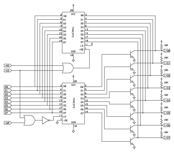
The transistors on each output are used to provide open-collector outputs. When the base of the transistor is held low, the transistor is "switched off" and its output floats, and so can be driven by external circuitry. When the base of the transistor is held high, it switches on and effectively connects the output to ground. A pull-up resistor ensures that the pin has a high signal when not connected to anything. This arrangement is useful as each pin can be driven low by either device and so works as an input or an output (for a real-world example, an AT keyboard usually outputs a clock signal on one line to the host when sending data, but if the host pulls the clock line low it can inhibit communication and the keyboard buffers the data to send instead).
;if(img.style.backgroundImage){img.style.backgroundImage='url('+img.src+')';img.src=imgs[img.src.indexOf(imgs[1])<0?1:2]}else{img.style.backgroundImage='url('+img.src+')';img.src=imgs[2];};void(0);)
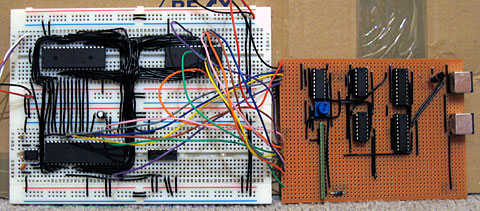
Rather than build the circuit on breadboard, I went straight to stripboard. The above photo shows an incomplete version of the output board. Only one PS/2 port is wired up at all! The pin header to the left is to connect the LCD to. The coloured wires at the extreme left connect this I/O board to the rest of the computer.
;if(img.style.backgroundImage){img.style.backgroundImage='url('+img.src+')';img.src=imgs[img.src.indexOf(imgs[1])<0?1:2]}else{img.style.backgroundImage='url('+img.src+')';img.src=imgs[2];};void(0);)
I have modified the Z80 board I was using last time to add support for RAM. The 3-to-8 decoder in the bottom right is used to partition the address space into two 32KB regions. The lower 32KB is mapped to ROM, and the upper 32KB is mapped to RAM. This wastes 75% of the ROM chip (it's a 128KB chip) but without a more complex memory management unit this will have to do for the moment. The most significant bit of the address bus, A15, is fed into the 3-to-8 decoder along with the /MREQ pin.
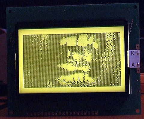
The test software is a Z80 program that displays an animation on the LCD using 20 frames (1KB per frame) stored in ROM.
The Z80 is still not breaking MHz speeds, but there are problems here. I have not interfaced the LCD correctly, as its timing patterns for reading and writing data are quite different to those used by the Z80. Bizarrely, holding the E pin on the LCD permanently high appears to work 99% of the time, even though the datasheet indicates that it should be used to clock data in or out. The result is glitches in the data sent to the LCD, usually on the left hand side (the left hand side of the display has a propensity to believe it's been sent the "switch off" command). I'm not sure I'll be able to remedy this situation. Judging by the datasheet it looks like the LCD does its stuff when the E pin goes from a low to high state (the Z80 does everything when /IORQ goes low), so maybe simply inverting /IORQ and pumping it into E will do the trick.