Laserstrike for Zen X-Fi 2
Sunday, 23rd October 2011
It's been a long time since I posted about any of my projects for the simple reason that I haven't had any real time to work on them this year. Work commitments have not been particularly kind to my free time and there has been no progress on my 3D engine for TI calculators or any new electronics projects.
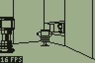
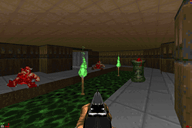
I did, however, replace my ailing Zen Xtra digital audio player with a Zen X-Fi 2 earlier in the year. The X-Fi 2 supports simple application development in Lua, a language I had no experience with, so I spent a few days in April knocking together a game as a learning project. I've always been fond of Kevin Ng's Laserstrike and it seemed a good fit for a device with a touch screen.
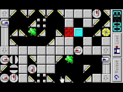
I used the smaller levels from Badga's Laser Mayhem as it let me use larger tiles, otherwise it would be tricky to tap the correct block on the X-Fi 2's 3" screen.
Having not used Lua before the code is far from brilliant (for some reason I chose to represent the level as a string rather than an array, by way of example) but it works well enough and has occasionally kept me occupied on bus and train journeys. Rather than let the game stagnate on my hard disk drive I added a final bit of polish and have released it on my website. If you'd like to try the game but do not own an X-Fi 2 (which would be almost everyone reading this) you can play it in the Zen X-Fi 2 Application Development Kit (extract the game to C:\Creative\ZEN X-Fi2\Applications) but be warned that the simulator is a little buggy (it doesn't detect touch input in the 16 rows and columns at the top and left edges of the screen for starters).
Fingers crossed I can get more time for what I enjoy doing in 2012. I have plenty of fun ideas, but little time to put them into practice!
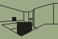
A larger level, moving sectors and failed optimisation attempts
Monday, 29th November 2010
I've made a few attempts to boost the performance of the 3D engine for the TI-83+ I'm working on with little success. I had previously failed to get any improvement by adding bounding boxes around each BSP node (the idea being that if a node falls outside the view you can discard it and, by extension, all of its children) but the act of transforming the bounding box to determine whether it was inside or outside the view was more CPU intensive than blindly handling the nodes whether they were inside the view or not.
A simpler test, I reckoned, would be to use bounding circles. These only have one point to transform, and determining whether they are in the view is one comparison to ensure that they're in front of the camera followed by one multiplication (by the constant √2) and two more comparisons to determine whether they are to the left or right of the camera's view; far simpler than a bounding box!
The bounding circles did cut down the number of BSP nodes that were handled each frame but the additional checks made the engine slightly slower in general than it had been before. In some circumstances it was slightly faster, but not enough to make a noticeable difference. The additional data per BSP node added over 900 bytes to the level data, too, so the attempted optimisation had to go.

The newly added rooms to the demo level
One tweak that did boost performance noticeably was to cache the projected X coordinate of each vertex. All vertices in the map have at least two walls connected to them and so are projected to the screen at least twice if within the view. I already had a table that was used to indicate whether a vertex had been transformed around the camera or not that frame so it was easy enough to add the X coordinate of the projected vertex to that table, adding around a 15% boost to the framerate.
Points are projected to the screen by dividing their X (left/right) or Z (up/down) component by their Y (depth) component. Division is slower than multiplication so I tried to calculate the reciprocal of the depth for the vertex then perform all subsequent projection operations by multiplying the X or Z component by this reciprocal. Unfortunately, this resulted in a lack of precision owing to my use of 16-bit fixed-point numbers (walls "wobbled" as you moved the camera) and performance was about the same as it had been before, so I rolled back the changes.
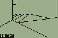
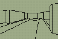
The block of screenshots in the above text shows a new region that has been added to the demo level, and the image below is a map of that level — fans of DOOM may notice that it's based on a small portion of E2M7 (The Spawning Vats).
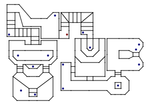
Map of the level
This level now uses every one of the 256 walls that are available, so is probably a good indication of the maximum size of a single level (and at 6,626 bytes it's certainly rather taxing on the limited amount of memory in a TI-83+ calculator).
This is, however, the maximum size of a single level. It does not take long to load and unload levels, so it would be quite possible to construct a continuous level that appears larger by unloading the current one and loading a different one when the user moves to a particular region. This could be implemented in an obvious manner (such as the player stepping into a teleporter) or transparently (by moving the player into an identical copy of the room he left to hide the transition). The latter option also introduces the option of level geometry that would otherwise be impossible in a 2D-based engine, such as rooms above rooms. Special effects could also be tried, such as an infinite corridor that warps you back to the beginning when you reach its end.
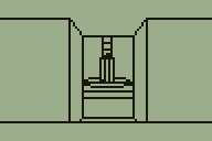
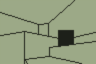
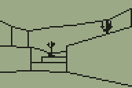
However this feature is implemented, there would need to be some way to trigger the action. The above animated screenshot demonstrates the current trigger system which is used to set a sector in motion. A sector, in this instance, is a region with a particular floor height and ceiling height. Each wall indicates which sector is in front of it and which sector is behind it. Convex sub-sectors contain sets of walls and also indicate which sector they are part of, and are attached to the leaves of the BSP tree. Given a point, you can quickly find out which convex sub-sector it is in by walking the BSP tree. When you have found the convex sub-sector you can then look up its sector. This is currently used to set the player's height, as the sector tells you the floor height.
If you keep track of the player's sector each frame you can tell when they have moved from one sector to another. This then fires an event, reporting which sector the player used to be in and which they are in now. In the above screenshot, the platform is set to descend whenever the sector surrounding it is entered from any sector other than the platform itself (this is to stop it from automatically descending when the player walks off the top of the raised platform). It is also set to rise whenever the platform's own sector is entered. This produces a simple lift; doors are handled in a similar fashion elsewhere in the level.
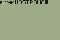
If you'd like to try this demo on your calculator, you can download the binaries for the TI-83 and TI-83+ in Nostromo.zip. As ever, please back up any important files on your calculator before running the demo; it may well clear your RAM. For those without calculators, an animated screenshot is available.
Collision detection makes the world feel solid
Sunday, 21st November 2010
One of the larger problems with the 3D engine for the TI-83+ calculator series I have been working on is that it's possible to move the camera through walls. This doesn't make the world feel especially solid, so I've started working on some collision detection routines.
Work commitments have left me with little time to spend on this project over the last couple of weeks so progress has been very slow, but I've got a basic collision detection system mostly working.

I spend most of the above screenshot running into walls. The code seems to work relatively well and quite quickly, though it's far from perfect. The still image shows the new settings screen, which is hopefully a little easier to use than remembering which keys do what. It also has the advantage of displaying the state of the current settings.
The walls are stored as line segments between two 2D vertices, and the collision detection has to ensure that the player does not get too close to any of these walls. The technique I have used starts by calculating the closest point on the line to the player.
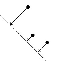
The above image shows a wall (the solid line segment) and three possible player positions (the heavy dots). The arrows point to the closest point on the wall's line. The closest point on the line to the top player position is past the end of the line segment, so it is ignored. The other two closest points lie on the line segment, so these are checked in more detail.
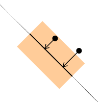
The distance between the closest point on the line and the player position is then calculated and compared to a threshold value (the radius of the player). The above image highlights the out-of-bounds region in tan. The lower player position is outside this region so is ignored, but the upper player position is inside it and needs to be corrected.
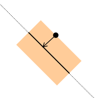
The correction is quite straightforward. We know the closest point on the wall to the player. The angle of the wall's normal is stored in the level file, so we can easily calculate a vector from that to push the player a fixed distance away from the wall.
In addition to the above 2D checks, a very simple height check is performed for "upper and lower"-type walls. These are walls with a central hole so you can pass over or under them, and are used to connect sectors with varying floor and ceiling heights. The top of the player's head is used to check the ceiling height. Rather than use the height of the player's feet to check the floor height their knee height is used. This is to allow the player to climb low walls (such as the edges of steps).
When I first implemented these collision detection techniques I checked every wall in the map. This halved the framerate in places, and as the framerate is not particularly high in the first place I needed to find a way to reduce the number of tests. Taking further inspiration from DOOM I implemented a "blockmap". This breaks the map down into square blocks and each block contains a list of which walls pass through it. To perform collision detection I look up which block the player is in and from that I can retrieve a reduced list of which walls they may end up walking into. The original implementation had to check well over a hundred walls for each movement; the blockmap reduces this to 26 in the worst case scenario for the current level design.
Sadly, this additional blockmap enlarged the size of the map quite a bit, so I've attempted to reduce it a little. For simplicity and performance most structures referred to other structures by pointer (for example a sub sector contained a list of pointers to walls and each wall contained pointers to a front and back sector). I've changed most of these to now refer to other structures by index, which shaved a few hundred bytes off the map at the cost of a few hundred clock cycles. Overall performance still isn't great, though I haven't found it noticeably slower than the previous demos.
I added very primitive physics for moving the player up and down relative to the floor to complement the collision detection. This retrieves the floor height from the sector directly under the centre of the player and compares it to the current player height. If the new floor height is higher than the old floor height then the player's foot height is set to a point half way between the two; this smoothes the animation slightly when climbing up stairs (rather than just snapping to the new floor height). When moving from a higher floor to a lower floor the player's downward speed is increased to roughly simulate gravity.
A demo for the TI-83+ series and TI-83 can be found in Nostromo.zip. As always, this is a piece of software in development and there may be calculator-crashing bugs, so please back up any important files before running it.
Enlarging the world
Sunday, 7th November 2010
There have been very few changes to the features of Nostromo recently. I have tried a number of ways to optimise the performance and whilst the handful of micro-optimisations I have made have boosted the frame rate a little none of the higher-level optimisations have done much. I did try, for example, storing a bounding box around each BSP node and ignoring it (and all its children) should this bounding box fall outside the field of view; the additional code to check the bounding box ended up halving the framerate rather than improving it.


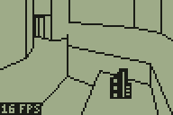
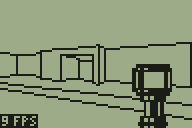

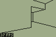
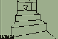
I have, however, enlarged the level quite considerably. A staircase connects the central room with the pit to a rather strangely-shaped arrangement of walls (again copied from E2M7). The room with a pit continues to cause issues; looking across it towards the room with the small central staircase forces the engine to step through a very large number of convex sub-sectors and check many walls. This drops the frame rate down to about 3 FPS on a TI-83+. However, this is specific to that room; the newly-added rooms have not noticeably affected the frame rate in other parts of the level.
Another minor improvement is that the engine now supports different sprites. I'm not too good at drawing them, as you can probably tell from the above screenshots, but at least the code is there to support them.
You can download a TI-83 and TI-83+ binary to try the demo on your calculator (please back up any important files first). Alternatively, here is an animated screenshot.
Adding sprite objects to the 3D world
Tuesday, 2nd November 2010
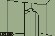
The previous entry showed a room from a map copied from DOOM's E2M7. I have since added the adjacent room:
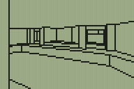
It may not look as interesting as the other room but it is significantly more costly to render due to the sheer number of lines visible at a time in it. Looking across it from the far corner dropped performance down to around 2 FPS on the 6MHz TI-83+, which was really not a very good effort. I spent a fair amount of time over the weekend trying to optimise the code as much as I could, and manage to bring the frame rate in the player's starting position from 6 FPS up to the target 10 FPS. Looking across the length of the new room still dropped the framerate to around 4 FPS at 6MHz, but it's a start.
Once the engine had been made a little faster it seemed a good idea to slow it back down again by adding a feature. I had been pondering how to add objects in the form of scaled sprites to the world. Working out where to put them on the screen isn't so difficult, but clipping them against the world geometry so that they couldn't be seen through walls is another matter entirely. One way that seemed popular is to draw the objects in reverse depth order (drawing the sprites that were further away before those that were closer) and using a depth buffer for the world geometry to clip each pixel of the sprite against the world. This would take up a lot of memory on the calculator and run very slowly (populating the buffer with a depth value for each pixel would be a very expensive operation, as you'd have to interpolate depth values between the ends of walls and edges of floors).
The engine makes use of three per-column clipping tables when rendering the scene. One keeps track of columns that have been completed (usually by drawing a "middle" wall to that column); once completed no more pixels may be drawn to that column. The other two tables are used to define the upper and lower clipping bounds. At the start of the scene these are reset to the top and bottom edges of the display. As the world is rendered from front-to-back these regions are reduced to clip geometry that is further away against geometry that is nearer (think of looking through a hole in a wall — things that are further away from you will never be drawn in the space above or below that hole).
Fortunately, you can use this clipping information to clip sprites against the world geometry too. Each sprite object needs to be associated with a convex subsector. These subsectors are made up of walls and are drawn from front-to-back (sorted by the BSP tree) as the world is rendered. Before each one of these subsectors is drawn it is checked to see if it contains any sprite objects — if it does, the current clipping buffers and a reference to the subsector are pushed onto a stack. When all of the walls and floors have been drawn this stack contains a list of all of the subsectors containing sprites and the clipping regions used to draw those subsectors in front-to-back order. Stacks are Last In, First Out structures and so when you pull the data back out of this stack you end up retrieving a list of sprites to draw and the associated clipping regions in back-to-front order. This allows you to effectively unwind the clipping operations, so as you draw the sprites from back-to-front you can gradually enlarge the clipping regions in the opposite order to the way that they were reduced when drawing the walls. You would still need to sort the sprites manually from back-to-front within each subsector, but for the time being I've limited myself to one sprite per subsector for ease of development.
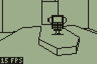
The above screenshots demonstrate an initial test of the "things" (as they are apparently technically called), rendering them as solid black squares.
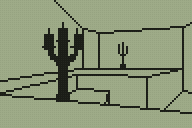
Scaled sprites tend to be more useful than solid black squares, however, so here are a pair of candlesticks (well, that was the intention at any rate; call them cacti if you must). The sprite was simply ORed to the display, so pixels could be black or transparent.
I then added support for "white" pixels too. The above screenshot is a link to an animated GIF showing the engine in action. The sprites appear to jiggle up and down and have invalid data drawn underneath them in places, which was caused by my accidentally overwriting an important register before rendering each column (fortunately an easy one to spot)! The relatively high frame rate in the above image was helped by running at 15MHz and using the old single-room map.
The above screenshot (click for the animated GIF) fixes the dancing sprites and restores the second room, though is still running at 15MHz. For a bit of fun I added animated doors; all this does is adjust the floor heights of the sectors used to represent "doors" (pressing Alpha will toggle both doors open or shut) but it makes the world look a little more dynamic.
There are still some rendering bugs in the engine. The above animated screenshot demonstrates one; when close to a wall edge you will sometimes see a temporary vertical line the height of the screen or the screen will flash white. I reckon this is probably an integer overflow issue causing the projected height of a line to be on the opposite side of the screen than the one it should be (the bottom edge of a hole in a wall may be projected above the screen rather than below it, causing the entire screen to be clipped out, for example). One bug that took a while to identify (it only appeared in very particular positions; moving one unit in any direction cured it) was caused by truncating a 32-bit integer to a 24-bit one. When viewing a long wall from a long distance the result of a 16-bit (difference between end and start X coordinates) by 16-bit (Y coordinate of the start of the wall) multiplication was resulting in a value of $00800000 or so (a large positive number). When truncated to 24 bits this becomes $800000, which has the most-significant bit set and was therefore treated as a large negative number. As this was part of the wall clipping code it would end up clipping a wall end a long way behind the camera instead of within the view; fortunately this obvious mistake is easy to spot and correct (the answer can only be positive, so if you get a negative one just negate it).
If you'd like to try the demo on your own calculator please download Nostromo.zip. As this is a work in progress there are likely to be bugs so please back up any important files first!