Text and filled shapes for the dsPIC33 VDC
Thursday, 22nd July 2010
The dsPIC33 video display controller project I am working on needs to support several common text output and drawing operations offered by existing BBC BASIC implementations. The previous demo included basic point, line and circle outlining functions, but I also need to output text and outline (or fill) rectangles, circles, ellipses and triangles. On top of that the drawing operations need to support multiple colours and plotting modes. Owing to processing power and memory limitations the output is black and white only but different "shades" can be implemented with dither patterns. The plotting modes allow you to perform logical operations between what you are drawing and what's currently on the buffer — for example, you could fill a circle that is logically ORed with the existing background or draw a line that inverts every pixel along its length rather than applying the new colour.
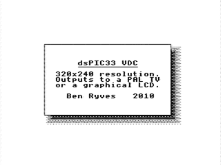
Filled rectangles and text output produce the above image.
Finding suitable algorithms for some of these routines has been a little tricky at times. Due to the way that filled shapes can be set to invert (rather than overwrite) what's on the background there has to be zero overdraw and the outline of filled triangles should exactly match the outline of a triangle drawn by plotting a line between its three vertices; this makes combining triangles to form more complex shapes possible, as you can guarantee that the overlap between the two shared vertices of a pair of triangles covers the same pixels as a line drawn between those two vertices.

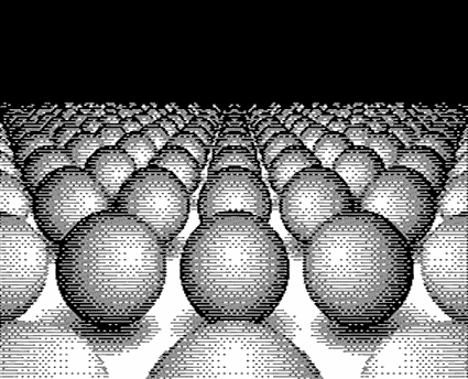
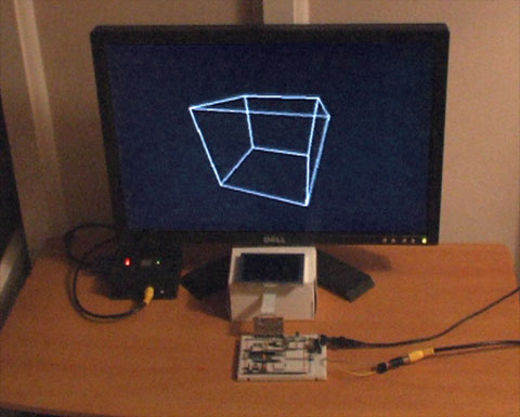
Filled triangles produce a solid cube.
I ended up writing a program in C# that would plot a random triangle using the triangle filler I was attempting to write and then compare its outline to that of a triangle drawn by plotting lines between the three vertices. The final code is chock full of special cases and workarounds but has been tested against hundreds of thousands of random triangles and seems to be working!
Due to a shortage of memory there is only a single frame buffer, which (naturally) means there is no double-buffering and hence smooth animation becomes a little tricky. When connected to a TV one can take advantage of the vertical blanking period to update the buffer (this is a period below and above the active display where you only need to feed sync signals, not image data, to the TV) and still get decent effects as long as you don't try to do too much. The LCD has no such vertical blanking period and so some of the demos look rather flickery.
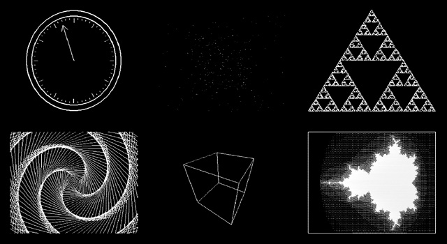
I have captured a video of the output of the circuit when running the demo which can be seen above. The horizontal grey lines are a limitation of my video capture card; these lines appear correctly as alternating black and white pixels on a real TV set! You can download the code for this demo from my site along with a PDF of the schematic. As this is a work in progress I'm sure there are plenty of bugs left to squash but I think it's getting there, slowly but surely!
360 degree photos from Lego, a PICAXE, C# and JavaScript
Friday, 9th July 2010
As you may have guessed from the ratio of photos to actual content in my entries I do quite enjoy taking photos of things. One of the reasons I enjoy working with electronics over writing software for computers is that a finished product results in something physical, which I find much more rewarding than a purely virtual hobby.
One type of photograph I particularly enjoy on other websites is the interactive 360° view of a product. The ability to click and drag to rotate an object on the screen makes it seem more real.
What do you need to take this sort of photograph and show it on a web page? There are four components I could think of:
- A rotating platform that could be controlled to rotate to a specific angle.
- A fixed camera that can be triggered once the platform has advanced to the correct angle.
- A way to combine all of the photos taken at different angles into a single file.
- An piece of code that would allow the user to rotate the object on-screen and display the correct single view of the object.
My final solution is a bit of a Heath Robinson affair but it seems to work quite well!
The rotating platform
The most obvious way to build such a platform is to use a stepper motor, as that is specifically designed to be positioned to a particular angle. The problem is that I don't have any stepper motors, and even if I did it would be quite tricky to connect one to a platform. A more practical alternative is to use something I do have — Lego Technic.
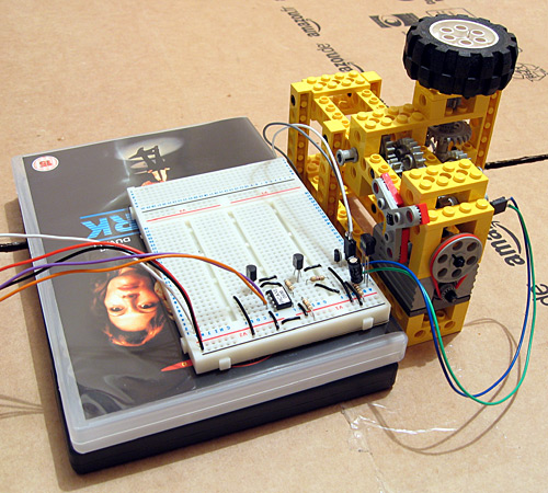
A Lego motor cannot be set to rotate to a particular position, so some additional electronics are required. The motor drives a worm gear which in turn rotates a three-bladed propeller relatively slowly (shown with red pieces attached to it in the photo). This propeller cuts the path of a beam of infra-red light between an LED and an infra-red receiver module. A microcontroller (in this case, a PICAXE-08M) is used to advance the platform in steps by switching the motor on, waiting for the beam to be unblocked, waiting for the beam to be blocked again then switching the motor off. The gears I am using have twenty-four or eight teeth, so each pair of gears divides the rotational speed by 24/8=3. I am using four pairs of gears which results in a division of 34=81. The propeller has three blades which further divides the rotational speed by three resulting in the ability to set the platform to 81×3=243 distinct angles.
' This code is for a PICAXE-08M
#PICAXE 08M

' This pin is used to generate the 38kHz IR carrier. It should be connected to the IR LED's cathode (-).
Symbol IRPwmPin = 2
' This pin is connected to the IR demodulator's output.
Symbol IRReceiverPin = Pin3

' This pin is connected to the motor enable output.
Symbol MotorPin = 4

Symbol SerialControlIn = 1

' The desired position of the "stepper" motor.
Symbol StepDesired = B8
' The current position of the "stepper" motor.
Symbol StepCurrent = B9

Symbol StepDesiredConfirm = B10
Symbol StepDesiredPotential = B11

' Returned from the CheckBeam routine.
Symbol BeamBlocked = B12

' Rather than spin once at a time (slow) spin up to this many times between exchanging position information with the computer.
Symbol SpinLoopCount = 3

' Stores the spin loop time.
Symbol SpinLoop = B13

' The number of steps in a complete revolution.
Symbol TotalSteps = 243


Main:

    ' Reset the current and desired steps.
    StepDesired = 0
    StepCurrent = 0

    ' Switch the motor off.
    Low MotorPin

    'StepDesiredConfirmCount = 0

    Do
        ' Fetch the desired position.
        SetFreq M8
        SerIn SerialControlIn, N4800_8, (CR, LF), #StepDesiredPotential, #StepDesiredConfirm
        SetFreq M4

        ' Check the received data - the second value should be the logical inversion of the first.
        StepDesiredConfirm = Not StepDesiredConfirm
        If StepDesiredPotential = StepDesiredConfirm Then
            StepDesired = StepDesiredPotential
        End If


        ' Adjust the position if required.
        For SpinLoop = 1 To SpinLoopCount

            ' Broadcast the current step position.
            SerTxd(#StepCurrent, ",", #StepDesired, CR, LF)

            ' Do we need to run the motor?
            If StepCurrent <> StepDesired Then

                ' Switch the motor on.
                High MotorPin
                Pause 20

                ' Wait for the beam to be unblocked.
                Do GoSub CheckBeam
                Loop Until BeamBlocked = 0


                Pause 20

                ' Wait for the beam to become blocked again.
                Do GoSub CheckBeam
                Loop Until BeamBlocked = 1

                ' Switch the motor off.
                Low MotorPin

                ' Increment step current to indicate a change of step.
                Inc StepCurrent
                If StepCurrent = TotalSteps Then
                    StepCurrent = 0
                End If
            End If


        Next SpinLoop

    Loop

' Checks whether the beam is blocked or not.
' Returns BeamBlocked = 0 for an unblocked beam, BeamBlocked for a blocked beam.
CheckBeam:
    PwmOut IRPwmPin, 25, 53 ' 38kHz, calculated via PICAXE->Wizards->pwmout
    Pause 1
    BeamBlocked = IRReceiverPin
    PwmOut IRPwmPin, Off
    Return
The BASIC program on the PICAXE constantly outputs the current position and desired position via the serial programming cable as ASCII in the format <current>,<desired><CR><LF>. It also checks for the desired position every loop on via a serial input pin (sadly not the one used for programming the PICAXE as that is not permitted on the 08M) in the format <CR><LF><desired>,<~desired>. (again in ASCII). The desired position is transmitted twice, once normally and the second time inverted (all zero bits set to one and all one bits set to zero) as a simple form of error detection; should the second value received not be a logical inversion of the first then the value is discarded.
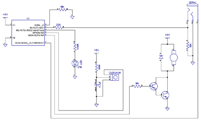
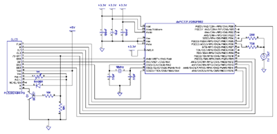
A copy of the schematic can be downloaded by clicking the above thumbnail. It is pretty simple; serial data is input on pin IN1 (move the serial input from the programming cable from SERIAL_IN to IN1), an IR LED is driven from pin PWM2 via a current-limiting resistor, an IR receiver sends its input to pin IN3, a Darlington pair drives the motor via pin OUT4 and information is sent out via the SERIAL_OUT pin (no need to move the programming cable for that one).
Triggering the camera
My camera does not have a standard remote control, but does has some software that allows you to capture shots when it's connected to your USB port. Unfortunately the Canon PowerShot SDK is rather old and is no longer maintained, which means that any software that uses it is bound to its bugs and limitations. One of its bigger problems is that it doesn't work on Vista; by setting the Remote Capture utility into XP compatibility mode I could set up a shot and see a live viewfinder but attempting to release the shutter caused the app to hang for about a minute before claiming the camera had been disconnected.
Fortunately VirtualBox emulates USB and serial ports so I set up Windows XP in a virtual machine and installed the Remote Capture utility. It still doesn't work very well (taking about thirty seconds between releasing the shutter and transferring the image) but it's better than nothing.
To control platform I use the following C# code. It's very poorly written (you need to make sure that you quickly set the Remote Capture application as the foreground window when you start it, for example, and it has a hard-coded 10 second delay after taking the photo to transfer the photo from the camera to the PC — when my camera's batteries started going flat it started to drop frames).
using System;
using System.Globalization;
using System.IO.Ports;
using System.Text;
using System.Text.RegularExpressions;
using System.Threading;
using System.Windows.Forms;
using System.Diagnostics;
using System.Linq;

class Program {

    const int StepsInRevolution = 243;

    enum ApplicationState {
        AligningStepper,
        WaitingStepperAligned,
        WaitingStartPistol,
        Photographing,
        Exiting,
    }

    static void Main(string[] args) {
        StringBuilder receivedData = new StringBuilder();
        using (var serialPort = new SerialPort("COM1", 4800, Parity.None, 8, StopBits.Two)) {
            serialPort.WriteTimeout = 1;

            serialPort.Open();

            var packetFieldsRegex = new Regex(@"^(\d+),(\d+)$");

            int? currentPosition = null;
            int desiredPosition = 0;
            int? confirmedDesiredPosition = null;
            int startPosition = 0;

            int angleCount = 64;
            int currentAngle = 0;

            serialPort.DataReceived += new SerialDataReceivedEventHandler((sender, e) => {
                if (e.EventType == SerialData.Chars) {
                    receivedData.Append(serialPort.ReadExisting());
                    string receivedDataString;
                    int newLinePosition;
                    while ((newLinePosition = (receivedDataString = receivedData.ToString()).IndexOf("\r\n")) != -1) {
                        var packet = receivedDataString.Substring(0, newLinePosition);
                        receivedData = receivedData.Remove(0, packet.Length + 2);
                        var packetFields = packetFieldsRegex.Matches(packet);
                        if (packetFields.Count == 1) {
                            currentPosition = int.Parse(packetFields[0].Groups[1].Value, CultureInfo.InvariantCulture);
                            confirmedDesiredPosition = int.Parse(packetFields[0].Groups[2].Value, CultureInfo.InvariantCulture);
                        }
                    }
                }
            });

            ApplicationState appState = ApplicationState.AligningStepper;

            // Main loop.
            while (appState != ApplicationState.Exiting) {
                // Update the stepper position.
                try {
                    serialPort.Write(string.Format(CultureInfo.InvariantCulture, "\r\n{0},{1}.", desiredPosition, (byte)~desiredPosition));
                } catch (TimeoutException) {
                    serialPort.DiscardOutBuffer();
                }
                Thread.Sleep(10);
                // What are we doing?
                switch (appState) {
                    case ApplicationState.AligningStepper:
                        if (currentPosition.HasValue) {
                            desiredPosition = (currentPosition.Value + 5) % StepsInRevolution;
                            appState = ApplicationState.WaitingStepperAligned;
                        }
                        break;
                    case ApplicationState.WaitingStepperAligned:
                        if (currentPosition.Value == desiredPosition) {
                            startPosition = desiredPosition;
                            appState = ApplicationState.WaitingStartPistol;
                            //while (Console.KeyAvailable) Console.ReadKey(true);
                            //Console.WriteLine("Press any key to start rotating...");
                        }
                        break;
                    case ApplicationState.WaitingStartPistol:
                        //while (Console.KeyAvailable) {
                        //  Console.ReadKey(true);
                            appState = ApplicationState.Photographing;
                        //}
                        break;
                    case ApplicationState.Photographing:
                        if (currentPosition == desiredPosition) {
                            Console.Write("Taking photo {0} of {1}...", currentAngle + 1, angleCount);
                            SendKeys.SendWait(" ");
                            Thread.Sleep(10000);
                            Console.WriteLine("Done!");
                            if (currentAngle++ == angleCount) {
                                appState = ApplicationState.Exiting;
                            } else {
                                desiredPosition = (startPosition + (currentAngle * StepsInRevolution) / angleCount) % StepsInRevolution;
                            }
                        }
                        break;
                }
            }

            Console.WriteLine("Done.");
            Console.ReadKey(true);
        }
    }
}
It was meant to prompt to press a key before starting to allow you to re-align the object to the starting position (if required) but this would switch focus away from the Remote Capture utility. I'll probably fix this to switch the focus explicitly to the Remote Capture utility before sending the key to trigger a capture, and will also add code that polls the photo destination directory to spot when the file has been downloaded from the camera instead of the hard-coded 10 second delay. Working in the virtual machine and with the buggy Remote Capture utility is a frustrating endeavour so I left it as it is for the time being!
Stitching the photos together
Once the photos had been taken they needed to be stitched together into a single file. I decided to use 64 angles for a complete revolution as this seemed a good trade-off between fine control over rotation and a decent file size. It also allowed the images to be arranged into a neat 8×8 grid.
I first used VirtualDub to crop each image. VirtualDub allows you to open an image sequence and export to an image sequence so it seemed ideal for the task. Once I had the object neatly cropped I stitched all of them together into a large single PNG file using the following C# program:
using System;
using System.Drawing;
using System.IO;
using System.Text.RegularExpressions;

class Program {
    static void Main(string[] args) {
        var middleImage = 14; // Index of the "middle" (default angle) image.
        var nameRegex = new Regex(@"Processed(\d{2})");
        var images = new Bitmap[64];
        try {
            foreach (var file in Directory.GetFiles(@"D:\Documents\Pictures\Digital Photos\Projects\Line Blanker\Insides 360\Processed", "*.png")) {
                var matches = nameRegex.Matches(file);
                if (matches.Count == 1) {
                    images[int.Parse(matches[0].Groups[1].Value)] = new Bitmap(file);
                }
            }
            var maxSize = new Size(0, 0);
            for (int i = 0; i < images.Length; i++) {
                if (images[i] == null) {
                    Console.WriteLine("Image {0} missing!", i);
                } else {
                    maxSize = new Size(Math.Max(images[i].Width, maxSize.Width), Math.Max(images[i].Height, maxSize.Height));
                }
            }
            using (var finalImage = new Bitmap(maxSize.Width * 8, maxSize.Height * 8)) {
                using (var g = Graphics.FromImage(finalImage)) {
                    g.PixelOffsetMode = System.Drawing.Drawing2D.PixelOffsetMode.Half;
                    for (int x = 0; x < 8; ++x) {
                        for (int y = 0; y < 8; ++y) {
                            var image = images[(x + y * 8 + middleImage) % images.Length];
                            if (image != null) {
                                g.DrawImage(image, new Point(x * maxSize.Width + (maxSize.Width - image.Width) / 2, y * maxSize.Height + (maxSize.Height - image.Height) / 2));
                            }
                        }
                    }
                }
                finalImage.Save("out.png");
            }
        } finally {
            for (int i = 0; i < images.Length; i++) {
                if (images[i] != null) {
                    images[i].Dispose();
                    images[i] = null;
                }
            }
        }
    }
}
The program requires that the input images are named Processed00.png to Processed63.png, which is easily arranged when exporting an image sequence from VirtualDub. The resulting image can be tidied up in a conventional image editor.
Embedding the result on a web page
The final bit of code required is to allow the 360° image to be embedded and manipulated on a web page. I opted to use JavaScript for this task as it seemed the lightest and simplest way to work.
if (typeof(Rotate360) == 'undefined') {
    var Rotate360 = new Class({
        Implements : [Options, Events],
        options : {
            width : 320,
            height : 240,
            container : null,
            element : null
        },
        sign : function(v) {
            return (v > 0) ? +1 : (v < 0 ? -1 : 0);
        },
        initialize : function(source, options) {
            this.setOptions(options);
            this.source = source;
            var rotate360 = this;
            this.element = new Element('div', {
                'class' : 'rotate360',
                styles : {
                    width : this.options.width + 'px',
                    height : this.options.height + 'px',
                    background : 'transparent no-repeat url("' + this.source + '") scroll 0 0'
                },
                events : {
                    mouseenter : function(e) {
                        if (typeof(rotate360.mouseHandlerDiv) != 'undefined') {
                            var myPosition = rotate360.element.getCoordinates();
                            rotate360.mouseHandlerDiv.setStyles({
                                left : myPosition.left + 'px',
                                top : myPosition.top + 'px',
                                width : myPosition.width + 'px',
                                height : myPosition.height + 'px'
                            });
                        }
                    }
                }
            });
            this.mouseHandlerDiv = new Element('div', {
                styles : {
                    position : 'absolute',
                    cursor : 'e-resize'
                },
                events : {
                    mousemove : function(e) {
                        if (typeof(rotate360.mouseHeld) != 'undefined' && rotate360.mouseHeld && typeof(rotate360.previousPageX) != 'undefined' && typeof(rotate360.previousPageY) != 'undefined') {
                            var currentBackgroundPosition = rotate360.element.getStyle('background-position').split(' ');
                            currentBackgroundPosition[0] = parseInt(currentBackgroundPosition[0]);
                            currentBackgroundPosition[1] = parseInt(currentBackgroundPosition[1]);
                            if (typeof(rotate360.rotateX) == 'undefined') rotate360.rotateX = 0;
                            rotate360.rotateX += (e.page.x - rotate360.previousPageX) / (360 * (rotate360.options.width / 270) / ((rotate360.image.width * rotate360.image.height) / (rotate360.options.width * rotate360.options.height)));
                            var workingAngle = parseInt(rotate360.rotateX);
                            currentBackgroundPosition[0] = -rotate360.options.width * (workingAngle % (rotate360.image.width / rotate360.options.width));
                            currentBackgroundPosition[1] = -rotate360.options.height * Math.floor(workingAngle / (rotate360.image.height / rotate360.options.height));
                            while (currentBackgroundPosition[0] > 0) currentBackgroundPosition[0] -= rotate360.image.width;
                            while (currentBackgroundPosition[0] <= -rotate360.image.width) currentBackgroundPosition[0] += rotate360.image.width;
                            while (currentBackgroundPosition[1] > 0) currentBackgroundPosition[1] -= rotate360.image.height;
                            while (currentBackgroundPosition[1] <= -rotate360.image.height) currentBackgroundPosition[1] += rotate360.image.height;
                            rotate360.element.setStyle('background-position', currentBackgroundPosition[0] + 'px ' + currentBackgroundPosition[1] + 'px');
                            rotate360.previousPageX = e.page.x;
                            rotate360.previousPageY = e.page.y;
                        } else {
                            rotate360.previousPageX = e.page.x;
                            rotate360.previousPageY = e.page.y;
                        }
                    },
                    mousedown : function(e) {
                        e.stop();
                        rotate360.mouseHeld = true;
                        rotate360.mouseHandlerDiv.setStyles({
                            left : 0,
                            width : '100%'
                        });
                    },
                    mouseup : function(e) {
                        e.stop();
                        rotate360.mouseHeld = false;
                        rotate360.element.fireEvent('mouseenter');
                    }
                }
            }).inject(document.body, 'top');
            this.image = new Asset.image(this.source, {
                onload : function() {
                    if (rotate360.options.element) {
                        rotate360.element.replaces(rotate360.options.element);
                    } else if (rotate360.options.container) {
                        rotate360.options.container.adopt(rotate360.element);
                    }
                }
            });
        }
    });
    window.addEvent('domready', function() {
        $$('img.rotate360').each(function(rotate360) {
            var src = rotate360.src.replace(/\.([a-zA-Z]+)$/, '_360.$1');
            var img = new Asset.image(src, {
                onload : function() {
                    new Rotate360(img.src, {
                        width : rotate360.width,
                        height : rotate360.height,
                        element : rotate360
                    });
                }
            });
        });
    });
}
The above code requires MooTools (both "core" and "more" for its Asset classes). It can be invoked manually or (preferably) will replace any image with a class of rotate360 with the 360° version — if the file was example.jpg the 360° version would be example_360.jpg.
Examples
I've taken photos of a few of my previous projects using this technique — USB remote control, AVR TV game and VGA line blanker. The process could use some refinement but it certainly seems to work!
dsPIC33 VDC with GLCD or PAL TV output
Sunday, 4th July 2010
I have currently been using some terminal emulation software on my PC to see the output of the Z80 computer. It seems a little silly to rely on a large multi-gigahertz, multi-megabyte machine just to display the output from a machine at the megahertz and kilobyte end of the scale. I had previously done some work with a dsPIC33 to drive a 320×240 pixel graphical LCD so dug out its breadboard and dusted off the code to try to make something of it.
Inspired by John Burton's recent experiments with PAL TV output I decided that the first thing I should do is add support for TV output. The graphical LCD is nice but a little small and responds to pixel changes rather slowly, making animation very blurry.
I think the results are reasonably good. A lot of the code is shared with the old LCD driving code, which means that the LCD demos work fine with the TV too. Fortunately, retracing the TV is a much less CPU-intensive job than retracing the LCD. The PIC has an SPI peripheral that allows you to clock out eight or sixteen bits a bit at a time at a selected speed by writing to a single register, which is great for clocking out the pixel data on each scanline. Even better are the PIC's DMA channels, which allow you to output a selected number of bytes or words to a selected peripheral from a specified location in RAM with no CPU involvement; all I need to do on each line is to copy a complete scanline to the DMA memory, initiate a transfer from this memory to the SPI peripheral and the job is as good as done. Using the DMA hardware as opposed to writing to the SPI registers directly reduced the rendering time of the Mandelbrot fractal part of the demo from 33 seconds to 18 seconds.
One problem I haven't been able to resolve is that the PIC inserts a small delay between every DMA/SPI transfer, which results in every sixteenth pixel being a bit wider than the fifteen before it. This is especially noticed on dithered regions. If I write to the SPI registers directly this delay vanishes. I'm not sure if the picture quality increase is worth the loss of performance, so I'd rather find a proper fix for this! For the time being, here's a video of the demo as it currently runs:
The TV contains a 75Ω resistor to ground on its composite video input. Two resistors are used on two PIC pins to form a voltage divider to produce the required output voltages (0V for sync, 0.3V for black and 1V for white). When the TV is disconnected the output of the circuit is 3.3V (the supply voltage, equivalent to a logic "high") as there's no load resistance to pull it to the correct 0.3V (a logic "low"). This can be used to periodically check whether a TV is connected and to switch between the LCD and TV output modes.
The above is rather vague, and I would recommend Rickard Gunée's article entitled How to generate video signals in software using PIC for more detailed information! The code for the demo can be downloaded from my website for those who are interested.
Update: I've updated my code to use the SPI peripheral in slave mode and use a timer and output compare unit to generate the clock signal. This regular clock signal produces pixels of identical sizes the new code can be downloaded here.
Booting CP/M 3 from an SD card
Wednesday, 23rd June 2010
Up to this point I have been running CP/M 2.2 on the Z80 computer. CP/M 3 adds a number of useful features, including the following:
- Support for more than 64KB RAM via banked memory.
- Standardised access to real-time clock for file date and time stamping.
- Improved text entry on the command-line when using the memory-banked version, such as the ability to move the cursor when editing and recall the previously entered line.
- Support for disks with physical sectors larger than the default record size of 128 bytes.
Switching to a banked memory system would require some new hardware in the form of a memory management unit so I have stuck with the simpler non-banked system for the time being. Support for physical disk sectors larger than 128 bytes is more interesting (SD cards use 512 byte "blocks") and real-time clocks are always useful so I have started working on updating to CP/M 3.
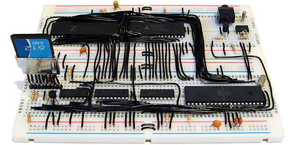
Z80 computer with new SD card slot (bottom left) and real-time clock (top right)
CP/M consists of three main pieces of software:
- A BIOS which exposes a small number of routines to perform primitive, hardware-specific operations (e.g. output a character to the console, read a raw sector from a disk, check if a key has been pressed).
- The BDOS which provides the main API for transient programs (e.g. read a complete line of input from the console, create a file, read a record from a file).
- The CCP, or console command processor, which provides the main user interface for loading and running other programs or performing some basic tasks via its built-in commands. This would be analogous to COMMAND.COM on DOS.
When working with CP/M 2.2 I had source files for these three pieces of software, so I just needed to implement the 17 BIOS functions, reassemble the three files to fixed addresses in memory and load them to these fixed addresses using the AVR when booting the computer. These three files were stored in the lower 8KB of the flash memory chip and were not accessible from within CP/M itself.
CP/M 3 proved to be a bit more of a challenge, as it is loaded slightly differently. The CCP is stored as a regular file named CCP.COM on the floppy disk you're booting from, so only the BIOS and BDOS need to be loaded from their hiding place at the start of the boot disk. These two pieces of software are merged into a single file named CPM3.SYS by a CP/M utility named GENCPM. To get this utility to work I needed to provide GENCPM with a hardware-specific BIOS3.SPR file that implemented the 31 BIOS routines. Fortunately, a file named BIOSKRNL.ASM is provided that implements most of the boilerplate code involved with writing a BIOS (you still have to provide the hardware-specific routines yourself, but your task is made much easier by following the template) so I just needed to recompile that for a non-banked system and link it with my handful of hardware-specific routines.
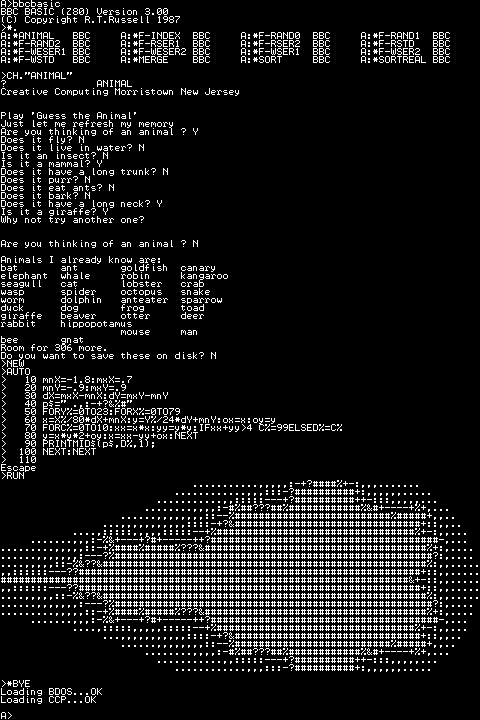
Ideally, CPM3.SYS would be stored on the regular file system with CCP.COM and the hidden boot loader would load CPM3.SYS for you. CP/M 3 does provide a small boot loader for this purpose (aptly named CPMLDR) which employs a cut-down BDOS and BIOS to load CPM3.SYS from the file system into memory for you. I haven't been able to get it to work, though, so I currently parse and load CPM3.SYS using some C code on the AVR. This works well enough for the time being, as can be seen in the above output generated by the computer when testing the real-time clock.
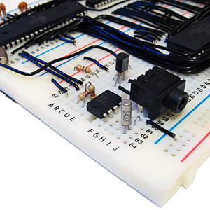
The time and date is maintained by a DS1307, an inexpensive eight-pin real-time clock and calendar chip that is shown in the middle of the above photograph. It is accessed over the I2C bus using a protocol that is natively supported by the AVR hardware. It uses binary-coded decimal to represent dates and times, which corresponds nicely to the time format used by CP/M; however, CP/M represents dates as a 16-bit integer counting the number of days since the 31st December 1977. I have used the algorithms on this website to convert dates to and from this format and the individual components.
The only downside of the DS1307 is that it only stores a two-digit year number, not the four digits one would hope for. This means that the century is discarded when setting the real-time clock, allowing for you to set a date that is then retrieved differently (truncated to the range 1930..2029). I haven't thought of a suitable solution to this problem just yet. I could use the AVR to act as the real-time clock, but I would then lose the advantage of the DS1307's battery backup that kicks in when the main power supply is removed.
The state of the DS1307 is effectively random at power-up. One of the first things the computer does when booting is to read the current date and time and check that all fields are within range. If not it resets them to midnight on the 1st January 1978 and displays a message to indicate that it has done so.
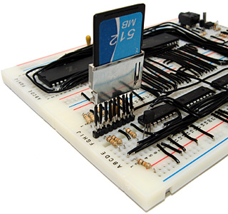
The SD card has been a bit of a headache to get working and though it currently only supports reading, not writing, it should hopefully be a useful addition to the computer. Rather than the previous arrangement of series rectifier diodes to drop the supply voltage and zener diodes to protect the inputs I'm using a dedicated 3.3V regulator to power the card and resistor voltage dividers to drop the 5V logic signals to around 3V (the closest I could get to 3.3V with the resistors I had to hand). I'm using the disk image from the old 512KB flash chip and treating the card as having 128 byte sectors so the arrangement is no more capable than before and in some cases quite a lot slower (reading a 128 byte record now entails reading a whole 512 byte block from the card then returning the desired 128 byte range within that block) but it seems to be as reliable as it used to be at least. SD cards append a CRC16 checksum when transferring data blocks so I can hopefully detect errors more easily and their on-board flash memory controller should perform wear-levelling, prolonging the life of the card.
To write the disk image to the card I used HxD which makes the job as easy as copy and paste. One problem I did have is that it displayed an "Access denied" error when attempting to write data, which I assume to be because something in Windows was using the card at the same time as HxD. I knocked together a short program for the AVR that wrote junk to the first block of the card, the result being that Windows no longer recognised the card's file system and HxD managed to write the data to the disk with no further problems.
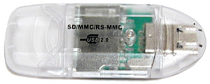
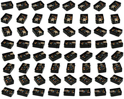
Sockets for regular SD cards seem to be relatively expensive for what they are, but the above SD card reader cost a pound (what else?) from Poundland. A bit of work with a soldering iron and some desoldering tools yielded some useful components:
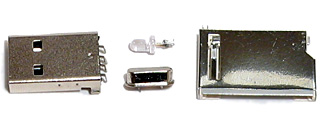
The crystal is unmarked and I'm hardly short of LEDs but the USB A connector could be a good way to reduce the size of a project that plugs into a USB port (USB B connectors are rather bulky) and the SD card slot works brilliantly for my needs here. There are cheaper and nastier ways to add an SD card slot to your project, but something like this feels more robust and has the advantage of reporting the state of the card's write protection switch.
Keyboard input and RAM disks make CP/M more useful
Wednesday, 16th June 2010
The hardware for the computer has changed in (mostly) subtle ways since the last post, with the exception of a PS/2 socket for connection to a keyboard.

PS/2 keyboards (which use the same protocol as the older AT keyboard) communicate with the host by clocking data in either direction (keyboard to host or host to keyboard) over two wires, appropriately named "clock" and "data". An AVR pin change interrupt is used to detect a change in state of the clock line and either input or output a bit on the data line depending on the current direction of data transmission. Incoming bytes generally relate to the scancode of the key that has just been pressed or released. These scancodes are looked up on a series of hard-coded tables to translate them into their corresponding ASCII characters. CP/M accesses the keyboard via two BIOS routines: CONST (2), which checks whether a character is available or not, and CONIN (3), which retrieves the character. I initially implemented these by simply reading from I/O port 2 (CONST) or port 3 (CONIN).
As keyboard input is polled, CP/M was wasting a lot of time reading from the AVR. Due to the AVR's relatively slow way to respond to I/O requests this was slowing down any program that needed to periodically call CONST (for example, BBC BASIC constantly checks for the Escape key when interpreting BASIC programs). I converted this polling system into an event driven one by connecting the AVR to the Z80's maskable interrupt pin, /INT. When a new key is received by the AVR it pulls /INT low to assert it. The Z80 responds to the interrupt request by setting an internal flag to remember that a key has been pressed and acknowledges the interrupt by outputting a value to port $38 (the Z80's maskable interrupt handler resides at a fixed address of $38 in memory, so this seemed like a sensible choice). The AVR detects this write to port $38 and returns /INT to its high state. The CONST routine can now directly return the value of this flag when polled (rather than having to request the flag from the AVR) which noticeably speeds up running programs. The flag is cleared when a key is read by calling CONIN.
I did have some difficulty getting the interrupt system to work; the Z80 has a number of different ways of responding to interrupts, two of which rely on fetching a value from the data bus by asserting /IORQ before an interrupt is serviced. IM 0 fetches an instruction from the bus and executes it, and IM 2 fetches the least significant byte of the address of the interrupt service routine to combine with the most significant byte stored in the I register. IM 1 (which is what I'm using) just jumps to the fixed address $38. However, I hadn't taken this additional data read into account and when the Z80 attempted to read from an I/O device the AVR was either putting nonsense on the bus or (deliberately) locking up with a message to indicate an unsupported operation. Fortunately you can easily tell the difference between a regular I/O request and an interrupt data request by checking the Z80's /M1 output pin, so with that addition things started working a bit more smoothly!
I'm still using terminal emulation software on my PC to view the output of the computer, though as I now have keyboard entry the results are a little more impressive than the few boot report lines and a prompt that were in the last entry. I still haven't worked out why my PC switches off or blue-screens when programming AVRs over the serial port, so I've soldered together a parallel port programmer for the time being.
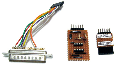
The pinout of the programmer matches that of the website where I found the SI Prog design. The ATmega644P's SPI, power and reset pins that the programmer interfaces with are all adjacent, but not in the same order as the ones in the SI Prog, hence the small board to the right of the above photo which swaps the pin order around using wires soldered to its reverse (this saves a lot of breadboard space). The board in the middle plugs directly into the parallel port programmer and is used to program the 512KB flash memory chip I'm using for storage.
I haven't got around to implementing writing to this flash memory yet, unfortunately, though I have implemented a simple way to test a writable disk drive. The RAM chip I am using is a 128KB one, as Farnell didn't sell 64KB ones. The Z80 can only address 64KB without additional memory banking hardware, so I'd simply tied A16 low and was ignoring half of the memory. I have now edited the BIOS to expose two disk drives; the default A: (512KB of flash memory) and now B:, a 64KB RAM drive. A16 is now driven by the AVR; during normal operation, it is held low (giving the Z80 access to its usual 64KB) but during disk operations it can be driven high to grant the AVR access to the previously hidden storage.
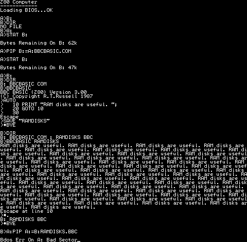
In the above test I use the STAT command to check free space, the PIP command to copy BBCBASIC.COM from A: (flash) to B: (RAM) then run BBC BASIC from the RAM disk, save a program then run it again by passing its filename as a command-line argument to BBC BASIC. At the end I try to copy the new program back to A:, but as there is no writing support for flash it keels over with a fairly unhelpful generic CP/M error.
Now that I've finally got something working in a vaguely usable manner, I hope I can start to research ways to make it better. Sorting out writing to flash would be a good start (I'm sorely tempted by jbb's suggestion to use an EEPROM to map logical floppy sectors to physical flash sectors) and I certainly hope to dig out my 320×240 pixel graphical LCD and driver for output instead of relying on a desktop PC. I'd also like to upgrade to CP/M 3 (I'm currently using CP/M 2.2) but when I last looked at that it seemed like a much more involved process so I decided to keep it simple. There's a fair mountain of stuff I need to take in, but I'm certainly learning a lot as I go (I only just realised tonight that CP/M was capable of graphics output, for one). I'd be a very happy chap if I could eventually run WordStar on this computer!