Emulators and neatened wiring
Tuesday, 12th August 2008
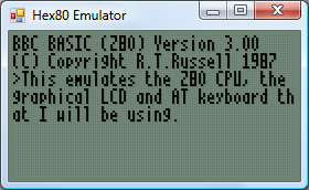
I've decided to switch to a regular 10MHz Z80 rather than a Z180, given the difficulty of using an SDIP 64. I now have a DIP 40 Z80 ready for use, but as I don't have the programmer for the Flash chip (which will hold the OS) there's not much I can do with it physically. I have therefore cobbled together a basic emulator to help develop some of the software beforehand.
To cut hardware costs I'm going to try and handle input in software. One bit of hardware I'm planning on having is an eight-bit open collector I/O port. Open collector pins float high in their reset state, and any device connected to the pin can drive it low. AT devices (keyboard and mouse) use this type of electrical connection, as does the I2C bus and the TI calculator link port. I can use up the eight pins easily - two pins per AT device (keyboard and mouse) makes four, two pins for the I2C bus and two pins for a TI calculator link port.
The I2C bus I mentioned above is a simple way to enhance the computer once built. There will be one device permanently attached to the bus, a DS1307 real-time clock, which will be used to provide time-keeping functions for the OS as well as generating periodic interrupts (the chip could be configured to trigger an interrupt 100 times a second, useful for timing game logic). I could then leave empty space on the circuit board to add other I2C devices over time, or have a socket on the case that could be used to plug in additional I2C modules.
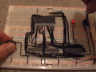
Now that I have some more tools, namely a desoldering pump, I tidied up the horrible hack job I'd done on the graphical LCD (replacing the multiple wires with a single pin header).
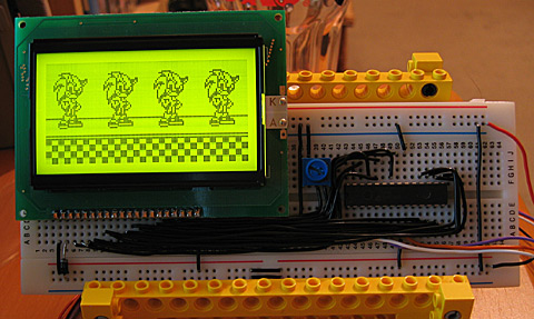
Yes, still the PICAXE here, but I'm using its 256 byte EEPROM to store a 32×64 pixel image of Sonic that is repeated four times horizontally.
I'm still not sure what I'm doing with regards to memory or storage. I'm still working on the simple assumption that ROM is 32KB ($0000..$7FFF) and RAM is 32KB ($8000..$FFFF) but this wastes a lot of memory and isn't very flexible at all. I've planned a bank-switching MMU, but as this will require at least four registers to store what appears in each of the four 16KB windows it will end up being physically very large and painful to wire.
As for storage, I have no idea. I have some 32KB I2C EEPROMs, but 32KB isn't exactly very large. Alternatively, I have an old 512MB SD card, and could try talking to it over bit-banged SPI. (SD cards use 3.3V, though, which complicates matters - not to mention that bit-banged SPI is going to be a little sluggish). I also have a USB module which can talk to USB mass storage devices over a serial connection, so maybe I should add a UART to the project. Adding a fully-blown USB module (which also plays WMA, MP3 and MIDI files) to such an otherwise low-tech computer feels like heresy, though.
Experimenting with a 32KB RAM
Monday, 4th August 2008
The next component I thought I'd experiment with is the RAM. The project is an analogue recorder - a circuit that samples an analogue input periodically and saves it in RAM, and can be configured to play the recorded signal back afterwards.
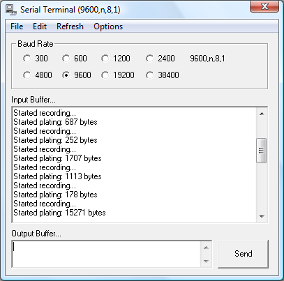
Yes, it says plating.
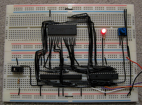
A single RAM chip offers 32K with an eight-bit word size. This requires fifteen lines to address it, A0..A14. The PICAXE-28X1 that is to control the circuit does not have enough output pins to be able drive this address bus and a data bus (to transfer values to and from RAM) and a still have enough pins left over to control the various components. To get around this, two octal (eight-bit) latches are used to drive the address lines, A0..A7 from one chip and A8..A14 from another. The inputs to these latches are connected to the data bus (PortC on the PICAXE), and two pins on the PICAXE are set aside to trigger the latch enable pins on either latch.
What this means in practice is that if you wished to change the current address to $1234 you would put $34 on the data bus and trigger the latch that corresponds to the least significant byte of the address, then put $12 on the data bus and trigger the latch that corresponds to the most significant byte of the address.
Any hobbyist can have wire insulation in any color that he wants so long as it is black.
A 10K potentiometer provides the required analogue input and an LED provides the output. The switch on the left is used to change between recording and playback modes. The large chip at the top is the RAM, the two small ones in the middle are the octal latches and the medium one on the right is the PICAXE-28X1.
As only 15 lines are needed to address 32KB, the most significant bit of the address bus is wired to the /WE pin of the RAM chip. This pin determines whether we're writing to (low) or reading from (high) the chip. This effectively means that addresses $0000..$7FFF are used when writing and addresses $8000..$FFFF are used when reading.
The only remaining connections to the RAM chip required are chip enable (/CE) and output enable (/OE). When chip enable is low, the RAM chip can be accessed; when high, it ignores all input. When not in use we therefore make sure that chip enable is high. When output enable is low, the RAM chip puts the value at the current address onto the data bus, so we need to pull this low when reading but make sure it's left high most of the time so that the RAM chip doesn't interfere with other devices trying to put a value on the data bus.
The code for the test program is as follows:
; Pins:
Symbol RamChipDisable   = 4
Symbol RamOutputDisable = 5
Symbol AddressLatch0    = 6
Symbol AddressLatch1    = 7

; Registers:
Symbol RamValue         = B0
Symbol RamAddress       = W1 ; B3:B2
Symbol RamAddressLow    = B2
Symbol RamAddressHigh   = B3
Symbol RamPointer       = W2 ; B5:B4

Symbol RecordingLength  = W3 ; B7:B6

Boot:
	Let DirsC = $00
	High RamChipDisable
	High RamOutputDisable
	Low AddressLatch0
	Low AddressLatch1
	Let RamPointer = 0
	SetFreq M8

Main:

StartPlaying:
	SerTxd ("Started playing: ", #RecordingLength, " bytes", CR, LF)
	Let RamPointer = 0
	Pause 100
PlayingLoop:
	If PortA Pin1 = 1 Then StartRecording

	; Read stored value from RAM.
	Let RamAddress = RamPointer
	GoSub ReadRam

	; Set LED brightness to stored value.
	Let W4 = RamValue * 4
	HPwm PwmSingle, PwmHHHH, %0100, 255, W4

	; Increment playback pointer and loop if hit end.
	Let RamPointer = RamPointer + 1
	If RamPointer = RecordingLength Then
		RamPointer = 0
	EndIf

	; Loop back.
	GoTo 	PlayingLoop


StartRecording:
	SerTxd ("Started recording...", CR, LF)
	Let RecordingLength = 0
	Pause 100
RecordingLoop:
	If PortA Pin1 = 0 Then StartPlaying

	; Read value from ADC.
	ReadAdc 0, RamValue

	; Set LED brightness to read value.
	Let W4 = RamValue * 4
	HPwm PwmSingle, PwmHHHH, %0100, 255, W4

	; Store value read from ADC into RAM.
	Let RamAddress = RecordingLength
	GoSub WriteRam

	; Increment record pointer.
	Let RecordingLength = RecordingLength + 1

	GoTo RecordingLoop

WriteRam:
	; Set up address bus:
	Let DirsC = $FF
	Let RamAddressHigh = RamAddressHigh & %01111111
	Let PinsC = RamAddressHigh
	High AddressLatch1 : Low  AddressLatch1
	Let PinsC = RamAddressLow
	High AddressLatch0 : Low  AddressLatch0
	; Set up data bus and write:
	Let PinsC = RamValue
	Low RamChipDisable
	High RamChipDisable
	Let DirsC = $00
	Return

ReadRam:
	; Set up address bus:
	Let DirsC = $FF
	Let RamAddressHigh = RamAddressHigh | %10000000
	Let PinsC = RamAddressHigh
	High AddressLatch1 : Low  AddressLatch1
	Let PinsC = RamAddressLow
	High AddressLatch0 : Low  AddressLatch0
	; Set up data bus and read:
	Let DirsC = $00
	Low RamOutputDisable
	Low RamChipDisable
	Let RamValue = Pins
	High RamChipDisable
	High RamOutputDisable
	Return
As before, there's a simple video of the circuit in action.
Back to Hardware
Friday, 1st August 2008
I enjoy dabbling with low-level programming, but have never actually built a computer to run these programs. I think it's time to correct that, and as the BBC BASIC project has required me to develop an almost complete Z80 OS (the only thing that's left for the TI-OS to do is manage files) I thought a Z80 computer would be a good start.
The planned specs are (as a starting point):
- 10 MHz Z80180 CPU;
- 64KB RAM (2 32K×8 SRAM chips);
- 128KB Flash ROM;
- Graphical LCD;
- Simple joypad input;
- Keyboard input (AT using either software AT routines or dedicated microcontroller).
The first spanner in the works is the Z80180, as I didn't read the datasheet closely enough and it's in a DIP 64 package with 0.07" pin spacing instead of the standard 0.1" pin spacing. I'll need to find some way of constructing an adapter so I can use it with my breadboards and stripboard. 
In the meantime, I've concentrated on the graphical LCD. I picked a 128×64 backlit graphical LCD for the princely sum of £16. It's very easy to control - you hook up it up to a 8-bit data bus to transfer image data and instructions and a handful of control pins to indicate what you're doing on that bus (reading or writing, whether you're sending an instruction or some image data, that sort of thing) and that's it - the only supporting circuitry it requires is a 10K potentiometer to act as a contrast control and power for the display and backlight.
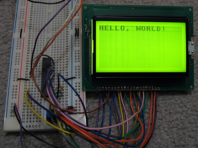
To experiment with the LCD, I'm using a PICAXE-28X1 microcontroller, programmed in BASIC. There isn't much space to store graphics, so I'm using a 32 character font (at eight bytes per character, that takes up all 256 bytes of free EEPROM space!)
; LCD data bus should be connected to port C.

Symbol LcdRegisterSelection = 0 ; D/I  :  4
Symbol LcdReadWrite         = 1 ; R/W  :  5
Symbol LcdStartEnable       = 2 ; E    :  6
Symbol LcdChipSelect1       = 3 ; CS1  : 15
Symbol LcdChipSelect2       = 4 ; CS2  : 16
Symbol LcdReset             = 5 ; /RST : 17

; Storage for console state variables.

Symbol ConsoleX             = B10
Symbol ConsoleY             = B11
Symbol ConsoleChar          = B12


	GoSub LcdInit                              ; Initialise LCD.
	B0 = %00111111 : GoSub LcdWriteInstruction ; Switch LCD on.

	GoSub LcdClear ; Clear LCD

	; Write the obligatory message to the LCD.

	ConsoleX = 0 : ConsoleY = 0

	ConsoleChar = $08 : GoSub LcdPutChar ; H
	ConsoleChar = $05 : GoSub LcdPutChar ; E
	ConsoleChar = $0C : GoSub LcdPutChar ; L
	ConsoleChar = $0C : GoSub LcdPutChar ; L
	ConsoleChar = $0F : GoSub LcdPutChar ; O
	ConsoleChar = $1D : GoSub LcdPutChar ; ,
	ConsoleChar = $00 : GoSub LcdPutChar ;
	ConsoleChar = $17 : GoSub LcdPutChar ; W
	ConsoleChar = $0F : GoSub LcdPutChar ; O
	ConsoleChar = $12 : GoSub LcdPutChar ; R
	ConsoleChar = $0C : GoSub LcdPutChar ; L
	ConsoleChar = $04 : GoSub LcdPutChar ; D
	ConsoleChar = $1B : GoSub LcdPutChar ; !

	Pause 2000

	B2 = 0
MainLoop:
	B2 = B2 - 1
	B0 = B2
	GoSub LcdGotoZ
	Pause 30
	GoTo MainLoop

LcdInit:
	DirsC = $00               ; Set data bus to input.
	High LcdStartEnable       ; We're not writing anything.
	High LcdChipSelect1
	High LcdChipSelect2
	Low LcdReset
	Pause 500
	High LcdReset
	Pause 500
	Return

LcdWriteInstruction:
	Low LcdReadWrite
	DirsC = $FF               ; Data bus = output.
	PinsC = B0                ; Set data bus state.
	Low LcdRegisterSelection  ; Instruction, not data.
	Low LcdStartEnable
	High LcdStartEnable
	DirsC = $00               ; Leave data bus floating.
	Return

LcdWriteData:
	Low LcdReadWrite
	DirsC = $FF               ; Data bus = output.
	PinsC = B0                ; Set data bus state.
	High LcdRegisterSelection ; Data, not instruction.
	Low LcdStartEnable
	High LcdStartEnable
	DirsC = $00               ; Leave data bus floating.
	Return

LcdGotoX:
	B0 = B0 And 7
	B0 = B0 + %10111000
	GoTo LcdWriteInstruction

LcdGotoY:
	B0 = B0 And 63
	B0 = B0 + %01000000
	GoTo LcdWriteInstruction

LcdGotoZ:
	B0 = B0 And 63
	B0 = B0 + %11000000
	GoTo LcdWriteInstruction

LcdClear:
	For B2 = 0 To 7
		B0 = B2
		GoSub LcdGotoX
		B0 = 0
		GoSub LcdGotoY
		B0 = 0
		For B3 = 0 To 63
			GoSub LcdWriteData
		Next
	Next B2
	Return

LcdPutMap:
	B1 = B0 * 8
	For B2 = 0 To 7
		Read B1, B0
		GoSub LcdWriteData
		B1 = B1 + 1
	Next B2
	Return

LcdPutChar:
	B0 = ConsoleY
	GoSub LcdGotoX
	B0 = ConsoleX * 8
	If B0 < 64 Then
		Low LcdChipSelect2
	Else
		Low LcdChipSelect1
		B0 = B0 - 64
	EndIf
	GoSub LcdGotoY
	B0 = ConsoleChar
	GoSub LcdPutMap
	High LcdChipSelect1
	High LcdChipSelect2
	ConsoleX = ConsoleX + 1
	If ConsoleX = 16 Then
		ConsoleX = 0
		ConsoleY = ConsoleY + 1
		If ConsoleY = 8 Then
			ConsoleY = 0
		EndIf
	EndIf
	Return

; Font
EEPROM $00,($00,$00,$00,$00,$00,$00,$00,$00,$7E,$7F,$09,$09,$7F,$7E,$00,$00)
EEPROM $10,($7F,$7F,$49,$49,$7F,$36,$00,$00,$3E,$7F,$41,$41,$63,$22,$00,$00)
EEPROM $20,($7F,$7F,$41,$63,$3E,$1C,$00,$00,$7F,$7F,$49,$49,$49,$41,$00,$00)
EEPROM $30,($7F,$7F,$09,$09,$09,$01,$00,$00,$3E,$7F,$41,$49,$7B,$3A,$00,$00)
EEPROM $40,($7F,$7F,$08,$08,$7F,$7F,$00,$00,$41,$41,$7F,$7F,$41,$41,$00,$00)
EEPROM $50,($20,$61,$41,$7F,$3F,$01,$00,$00,$7F,$7F,$1C,$36,$63,$41,$00,$00)
EEPROM $60,($7F,$7F,$40,$40,$40,$40,$00,$00,$7F,$7F,$06,$1C,$06,$7F,$7F,$00)
EEPROM $70,($7F,$7F,$0C,$18,$7F,$7F,$00,$00,$3E,$7F,$41,$41,$7F,$3E,$00,$00)
EEPROM $80,($7F,$7F,$09,$09,$0F,$06,$00,$00,$3E,$7F,$41,$31,$6F,$5E,$00,$00)
EEPROM $90,($7F,$7F,$09,$19,$7F,$66,$00,$00,$26,$6F,$49,$49,$7B,$32,$00,$00)
EEPROM $A0,($01,$01,$7F,$7F,$01,$01,$00,$00,$3F,$7F,$40,$40,$7F,$3F,$00,$00)
EEPROM $B0,($1F,$3F,$60,$60,$3F,$1F,$00,$00,$7F,$7F,$30,$1C,$30,$7F,$7F,$00)
EEPROM $C0,($63,$77,$1C,$1C,$77,$63,$00,$00,$07,$0F,$78,$78,$0F,$07,$00,$00)
EEPROM $D0,($61,$71,$59,$4D,$47,$43,$00,$00,$00,$00,$5F,$5F,$00,$00,$00,$00)
EEPROM $E0,($02,$03,$59,$5D,$07,$02,$00,$00,$00,$80,$E0,$60,$00,$00,$00,$00)
EEPROM $F0,($00,$00,$60,$60,$00,$00,$00,$00,$07,$07,$00,$07,$07,$00,$00,$00)
The code isn't very robust - it doesn't check the state of the LCD's busy flag as I'm assuming that a 4MHz PIC running an interpreted BASIC is too slow to manage to write another byte to the LCD driver before it has finished processing the last one.
The font was generated from the following image (it's the BBC Micro font):
It's rotated through 90° as, unlike the LCD driver in the TI-83+, each byte written outputs 8 pixels vertically, with the least significant at the top. (On the TI-83+, each byte written outputs 8 pixels horizontally, with the most significant bit on the left). More interestingly, this graphical LCD is made up of two 64×64 regions next to eachother, and by controlling two chip select pins you can control whether each byte written updates the left side, the right side, neither or both. I'm entirely sure how I could use this, though, other than not-very-exciting tricks like clearing the LCD extra-fast.
Finally, here's a video of the LCD test in action. It's not very speedy, but will hopefully pick up some speed once I figure out how I'm going to use that Z80180 CPU.
Subscribe to an RSS feed that only contains items with the PICAXE-28X1 tag.