C# emu2413
Thursday, 8th January 2009
This is fairly embarrassing; somebody sent me an email that was flagged as spam which I accidentally deleted. So if you sent me an email and I haven't replied, I'm not deliberately being rude; could you send it again? 
After encountering strange crashes (not .NET exceptions, full out crashes) with emu2413 I decided to port it to straight C# instead from its existing C incarnation (emu2413.h.cs and emu2413.c.cs). Even though the original was macro-heavy it was relatively simple to port, and so there's no dependency on an unmanaged DLL to generate FM sound any more. However, the C# version is significantly slower (Cogwheel now takes about 50% extra CPU time when FM sound is enabled), possibly due to many extraneous method calls that were macros in the original.
However, the emulator still crashes when FM sound is enabled. And I have no idea why, as it only happens in Release mode and outside the IDE. The Debug build works fine inside and outside the IDE, and Release mode works fine when run within the IDE. 
Controller input updates to Cogwheel
Monday, 5th January 2009
I hope you all had a good Christmas and New Year period!
I received an Xbox 360 controller for Christmas, so have done a bit of work on Cogwheel to add support for it. (You can download a copy of the latest version 1.0.2.0 with SlimDX here).
The first issue to deal with was the D-pad on the Xbox 360 controller. When treated as a conventional joystick or DirectInput device the D-pad state is returned via the point-of-view (POV) hat. The joystick input source class couldn't raise events generated by the POV hat so support for that had to be added. This now allows other controllers that used the POV hat for slightly bizarre reasons (eg the faceplate buttons on the PlayStation controller when using PPJoy) to work too.
The second issue was the slightly odd way that the Xbox 360's DirectInput driver returns the state of the triggers - as a single axis, with one trigger moving the axis in one direction, the other trigger moving it in the other. You cannot differentiate between both triggers being held and both being released, as both states return 0. To get around this, I've added support for XInput devices, where all buttons and triggers operate independently.
The Xbox 360 controller now shows up twice in the UI - once as an XInput device and again as a conventional joystick. Fortunately, you can check if a device is an XInput device by the presence of IG_ in its device ID. Here's some C# code that can be used to check with a joystick is an XInput device or not.
using System.Globalization;
using System.Management;
using System.Text.RegularExpressions;

namespace CogwheelSlimDX.JoystickInput {

    /// <summary>
    /// Provides methods for retrieving the state from a joystick.
    /// </summary>
    public class Joystick {

        /* ... */

        /// <summary>
        /// Gets the vendor identifier of the <see cref="Joystick"/>.
        /// </summary>
        public ushort VendorId { get; private set; }

        /// <summary>
        /// Gets the product identifier of the <see cref="Joystick"/>.
        /// </summary>
        public ushort ProductId { get; private set; }

        /* ... */

        /// <summary>
        /// Determines whether the device is an XInput device or not. Returns true if it is, false if it isn't.
        /// </summary>
        public bool IsXInputDevice {
            get {
                var ParseIds = new Regex(@"([VP])ID_([\da-fA-F]{4})"); // Used to grab the VID/PID components from the device ID string.

                // Iterate over all PNP devices.
                using (var QueryPnp = new ManagementObjectSearcher(@"\\.\root\cimv2", string.Format("Select * FROM Win32_PNPEntity"), new EnumerationOptions() { BlockSize = 20 })) {
                    foreach (var PnpDevice in QueryPnp.Get()) {

                        // Check if the DeviceId contains the tell-tale "IG_".
                        var DeviceId = (string)PnpDevice.Properties["DeviceID"].Value;
                        if (DeviceId.Contains("IG_")) {

                            // Check the VID/PID components against the joystick's.
                            var Ids = ParseIds.Matches(DeviceId);
                            if (Ids.Count == 2) {
                                ushort? VId = null, PId = null;
                                foreach (Match M in Ids) {
                                    ushort Value = ushort.Parse(M.Groups[2].Value, NumberStyles.HexNumber);
                                    switch (M.Groups[1].Value) {
                                        case "V": VId = Value; break;
                                        case "P": PId = Value; break;
                                    }
                                }
                                if (VId.HasValue && this.VendorId == VId && PId.HasValue && this.ProductId == PId) return true;
                            }
                        }
                    }
                }
                return false;
            }
        }

        /* ... */
    }
}
When the joysticks are enumerated they are only added to the input manager if they are not XInput devices.
To round up the entry, here's a screenshot of a minesweeper clone I've been working on in BBC BASIC.

You can view/download the code here and it will run in the shareware version of BBC BASIC for Windows. The code has been deliberately uglified (cramming multiple statements onto a single line, few comments, trimmed whitespace) to try and keep it within the shareware version's 8KB limit as this is a good limit to keep in mind for the TI-83+ version too.
Sega Master System emulation in Silverlight
Monday, 15th December 2008
I've had to quickly learn Silverlight for work recently, which has been an interesting experience. I've had to write new code, which is fine but doesn't really excite me as far as Silverlight is concerned - it doesn't really matter which language new code is developed in, as long as it gets the job done.
What does interest me more is that Silverlight is ".NET in your browser", and I'm a big fan of .NET technology with a handful of .NET-based projects under my belt. Silverlight therefore gives me the opportunity to run these projects within the browser, which is a fun idea. 
To this end, I've turned Cogwheel, a Sega 8-bit system emulator, into a Silverlight application. It took about an hour and a half, which was not as bad as I'd expected! (Skip to the bottom for instructions for the demo).
Raster graphics
Silverlight's raster graphics support is somewhat lacking. You can display raster graphics in Image elements, but - as far as I can see - that's about it. If you wish to generate and display images dynamically via primitive pixel-pushing, you're out of luck as far as Silverlight's class library is concerned.
Thankfully, Ian Griffiths has developed a class named PngGenerator that can speedily encode a PNG from an array of Colors that can then be displayed in an Image. Cogwheel's rasteriser returns pixel data as an array of integers so there's a small amount of overhead to convert these but other than that it's easy to push pixels, albeit in a fairly roundabout manner.
Render loop
The render loop is based around an empty Storyboard that invokes an Action every time it completes then restarts itself.
using System;
using System.Windows;
using System.Windows.Media.Animation;

namespace Cogwheel.Silverlight {

    public static class RenderLoop {

        public static void AttachRenderLoop(this FrameworkElement c, Action update) {
            var Board = new Storyboard();
            c.Resources.Add("RenderLoop", Board);
            Board.Completed += (sender, e) => {
                if (update != null) update();
                Board.Begin();
            };
            Board.Begin();
        }

        public static void DetachRenderLoop(this FrameworkElement c) {
            var Board = (Storyboard)c.Resources["RenderLoop"];
            Board.Stop();
            c.Resources.Remove("RenderLoop");
        }

    }
}
I'm not sure if this is the best way to do it, but it works well enough and is easy to use - just grab any FrameworkElement (in my case the Page UserControl) and call AttachRenderLoop:
private void UserControl_Loaded(object sender, RoutedEventArgs e) {
    this.UserControlRoot.AttachRenderLoop(() => {
        /* Update/render loop in here. */
    });
}
Missing .NET framework class library features
This is the big one; Silverlight does not cover the entire .NET framework class library, and so bits of it are missing. Fortunately this can be resolved, the difficulty depending on how you want the functionality of the original app to be affected.
Missing types you're not interested in.
These are the easiest to deal with, and this includes attributes and interfaces that the existing code uses that you're not especially interested in. For example, Cogwheel uses some of .NET's serialisation features for save states - a feature I wasn't intending on implementing in the Silverlight version. The [Serializable] and [NonSerialized] attributes are not available in Silverlight, nor is the IDeserializationCallback interface. To get the project to compile some dummy types were created.
namespace System {

    class SerializableAttribute : Attribute { }
    class NonSerializedAttribute : Attribute { }

    interface IDeserializationCallback {
        void OnDeserialization(object sender);
    }

}
Missing types or methods that you don't mind partially losing.
Cogwheel features some zip file handling code that uses System.IO.Compression.DeflateStream, a class not available in Silverlight. Rather than remove the zip classes entirely (which would require modifications to other files that relied on them) it was easier to use conditional compilation to skip over the DeflateStream where required.
switch (this.Method) {
    case CompressionMethod.Store:
        CompressingStream = CompressedStream;
        break;

    #if !SILVERLIGHT
    case CompressionMethod.Deflate:
        CompressingStream = new DeflateStream(CompressedStream, CompressionMode.Compress, true);
        break;
    #endif

    default:
        throw new NotSupportedException();
}
Missing instance methods.
C# 3.0 adds support for extension methods - user-defined methods that can be used to extend the functionality of existing classes that you cannot modify directly. Silverlight is missing a number of instance methods on certain classes, such as string.ToLowerInvariant();. By using extension methods the missing methods can be restored.
namespace System {

    public static class Extensions {
        public static string ToLowerInvariant(this string s) { return s.ToLower(CultureInfo.InvariantCulture); }
        public static string ToUpperInvariant(this string s) { return s.ToUpper(CultureInfo.InvariantCulture); }
    }

}
Missing static methods.
These are the most work to fix as extension methods only work on instance methods, not static methods. This requires a change at the place the method is called as well as the code for the method itself.
I've got around this by creating new static classes with Ex appended to the name then using using to alias the types. For example, Silverlight lacks the Array.ConvertAll method.
namespace System {

    static class ArrayEx {
        public static TOut[] ConvertAll<TIn, TOut>(TIn[] input, Func<TIn, TOut> fn) {
            TOut[] result = new TOut[input.Length];
            for (int i = 0; i < input.Length; i++) {
                result[i] = fn(input[i]);
            }
            return result;
        }
    }

}
First, a replacement method is written with Ex appended to the class name. Secondly, any file that contains a reference to the method has this added to the top:
#if SILVERLIGHT
using ArrayEx = System.ArrayEx;
#else
using System.IO.Compression;
using ArrayEx = System.Array;
#endif
Finally, anywhere in the code that calls Array.ConvertAll is modified to call ArrayEx.ConvertAll instead. When compiling for Silverlight it calls the new routine, otherwise it calls the regular Array.Convert.
Demo
The links below launch the emulator with the selected ROM image.
To run your own ROM image, click on the folder image in the bottom-right corner of the browser window to bring up a standard open file dialog.
Zip files are not handled correctly, but if you type *.* into the filename box, right-click a zip file, pick Open, then select the ROM from inside that it should work (it does on Vista at any rate).
The cursor keys act as you'd expect; Ctrl or Z is button 1/Start; Alt, Shift or X is 2 (Alt brings up the menu in IE). Space is Pause if you use an SMS ROM and Start if you use a Game Gear ROM. Keys don't work at all in Opera for some reason, but they should work fine in IE 8 and Firefox 3. You may need to click on the application first!
Issues
There are a number of issues I have yet to address. Performance is an obvious one; it's a little choppy even with 100% usage of one the cores on a Core 2 Duo. Sound is missing, and I'm not sure what Opera's doing with keys. Other than that, I thought it was a fun experiment.
Once I've tidied it up a bit I'll merge the source code with the existing source repository.
Virtual screen resolutions for BBC Micro compatibility
Monday, 8th December 2008
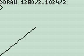
The BBC Micro had a virtual resolution of 1280×1024, meaning that if you drew a circle centred on (1280/2,1024/2) it would appear in the middle of the screen regardless of its pixel resolution. On top of that, (0,0) was in the bottom-left hand corner of the screen with the Y axis pointing upwards.
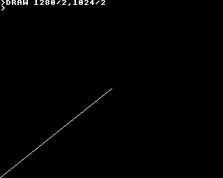
Thus far I'd been using the slightly more intuitive fixed resolution of 96×64 with (0,0) in the top-left hand corner with the Y axis pointing downwards. This means that any graphics program for the TI-83+ version appears upside down and squashed into the bottom-left corner when run on the BBC Micro.
I have worked on attempting to remedy this. 1280×1024 does not divide cleanly into 96×64, so I've used a constant scale factor of 16 on both axes resulting in a virtual resolution of 1536×1024. (Flipping the Y axis is easy enough). This means that programs drawing shapes (lines, circles, triangles, rectangles, parallelograms) will run on both BBC Micro "compatible" versions of BBC BASIC and the TI-83+ and produce roughly the same results.
As this may not be to everyone's tastes the two options may be independently controlled with two new star commands;
- *YAXIS UP|DOWN
- *GSCALE ON|OFF
The default is to have *YAXIS UP and *GSCALE ON. To revert to the old behaviour you could specify *YAXIS DOWN and *GSCALE OFF.
I have also been working on implementing the OS call OSGBPB. This call allows you to read/write multiple bytes of data in one go, so is much faster than using the byte-at-a-time BGET# and BPUT# commands. It also provides a way to enumerate filenames, a feature I have yet to implement but one that should be useful (eg to search for data files for your own program without having the filename hard-coded or having to prompt the user).
Three sides good, four sides bad.
Sunday, 30th November 2008
Work on the TI-83+/TI-84+ port of BBC BASIC continues bit-by-bit.


I've added triangle filling (left) and, by extension, parallelogram filling (right) PLOT commands. The triangle filler is a little sluggish, tracing each edge of the triangle using 16-bit arithmetic, but it seems fairly robust. I am trying to focus on robustness over speed for the moment, but it would seem easy enough to add a special-case triangle edge tracer if both ends of the edge can fit into 8-bit coordinates (all inputs to plot commands use 16-bit coordinates).
The parallelogram on the right is specified with three coordinates, and the fourth point's position is calculated with point3-point2+point1. As parallelograms are drawn as two triangles there's an overdraw bug when they are drawn in an inverting plotting mode.

This needs to be fixed.
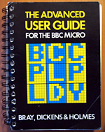
The BBC Micro OS exposed certain routines in the &FF80..&FFFF address range. These routines carried out a wide variety of tasks, from outputting a byte to the VDU to reading a line of input or changing the keyboard's auto-repeat rate. BBC BASIC (Z80) lets the person implementing the host interface catch these special-case calls, so I've started adding support for them. A friend very kindly donated copies of three BBC Micro books, including the advanced user guide (documenting, amongst other things, the OS routines) and the BASIC ROM manual.
 As an example, if you write the value 16 to the VDU it clears the text viewport. BBC BASIC has the CLS keyword for this, but you can also send values directly to the VDU with the VDU statement, like this: VDU 16. This in turn calls the BBC Micro's OSWRCH routine, located at &FFEE, with the accumulator A containing the value to send to the VDU. An alternative method to clear the text viewport would therefore be A%=16:CALL &FFEE.
Now, you may well be wondering how this is of any use, given the existance of a perfectly good CLS statement (or, failing that, the VDU statement). The usefulness becomes apparent when you remember that BBC BASIC has an inline assembler. There is no CLS or VDU instruction in Z80 assembly, but by providing an OSWRCH routine you can interact with the host interface and so clear the screen from an assembly code routine; in this case [LD A,16:CALL &FFEE:] (square brackets delimit assembly code).
Sadly, there is a limitiation in the TI-83+/TI-84+ hardware that prevents this from working seamlessly. The memory in the range &C000..&FFFF, where these routines reside, is mapped to RAM page 0. RAM page 0 has a form of execution protection applied to it, so if the Z80's program counter wanders onto RAM page 0 the hardware triggers a Z80 reset. To this end all of these OS calls are relocated to &4080..&40FF, so in the Z80 assembly snippet above you would CALL &40EE instead. This only applies to CALLs made from assembly code - the BASIC CALL statement traps calls to the &FF80..&FFFF so they can be redirected seamlessly to retain compatibility with other versions of BBC BASIC (Z80).
After all this work I noticed that the host interface was crashing in certain situations, especially when writing to a variable-sized file in a loop. This is the sort of bug that is tricky to fix; sometimes it would crash instantly, sometimes it would write the first 5KB of the file fine then crash.
It turned out to be a bug in the interrupt service routine (ISR). In this application the ISR is used to handle a number of tasks such as trapping the On key being pressed to set the Escape condition or to increment the TIME counter (as well as other time-related features such as the keyboard auto-repeat or cursor flash). On the TI-83+, which doesn't have a real-time clock, it also calls a RTC.Tick function approximately once per second to update the (very inaccurate) software real-time clock. To call this function it uses the BCALL OS routine. It appears that if the BCALL routine was used from an ISR when the TI-OS was in the process of enlarging a file it would crash. Removing the call to RTC.Tick appears to have fixed the bug entirely.

It is possible to put BBC BASIC into an infinite loop if you make a mistake in your error handler. In the above example program the error handler in line 10 fails to bail out on an error condition, running back into line 20 that itself triggers a division by zero error. You cannot break out of the loop by pressing On as that works by triggering an error (error 17, Escape). To improve safety I've added a feature whereby holding the On key down for about 5 seconds causes BBC BASIC to restart. This loses the program that was previously loaded in RAM, but you can retrieve with the OLD statement.
I've also rewritten all of the "star" commands. These are commands, usually prefixed with an asterisk, that are intended to be passed to the OS. As the TI-83+/TI-84+ does not have an especially useful command-line driven interface (most of the UI is menu-driven) I've implemented this part myself, basing its commands on ones provided by the BBC Micro OS. For example, *SAVE can be used to save a block of memory to a file, or *CAT (aliased to *DIR and *.) can be used to show a list of files.

In the case of *CAT I've added a pattern-matching feature that lets you use ? and * as wildcards to limit the files shown.
After noticing that *COPY took three seconds to copy an 860 byte file I optimised some of the file routines to handle block operations more efficiently. Reading and writing single bytes at a time is still rather sluggish, but I'm not sure that there's much I can really do about that.

Finally, for a bit of fun I noticed a forum post enquiring about writing assembly programs on the calculator. Here's a program that assembles a regular Ion program using BBC BASIC's assembler.