Building your own analogue sensors for the SmartBox
Friday, 29th November 2024
This is an extremely belated followup to a post from November last year, though one of the reasons for the delay was repeatedly being sent the wrong electronic components which ultimately led to the post from December. I'll try to explain as best I can...
Towards the end of last year I bought myself a SmartBox, a computer control system that's based around a 65C02 CPU and that runs programs written in an interpreted BASIC-like programming language, with software uploaded via a computer's serial connection (and once the programs are loaded onto the box, the serial connection can be severed and the program will continue to run). In the previous journal entry I focussed more on the software side, though to get practical use out of the box I had experimented with some of the hardware too and had built some analogue sensors that I was hoping to write up for the benefit of anyone else who'd acquired a SmartBox but none of the sensors to go with it.

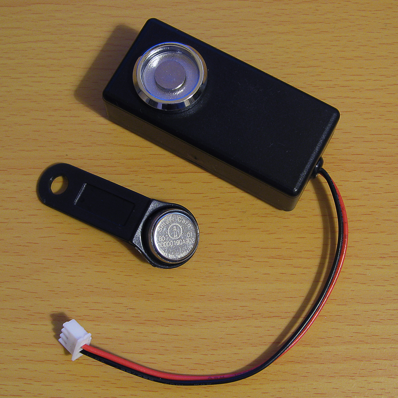
Two home-made User Adaptors and two home-made temperature sensors.
The four analogue sensor ports on the side of the SmartBox use 5-pin DIN sockets (180° to differentiate them from the 240° 5-pin DIN socket used for the serial port). Each sensor port can measure an analogue value with an 8-bit resolution (between 0 and 255) with the maximum voltage refererence being set to 2.55V – that is, each unit in the 0–255 range reported by the sensor corresponds to 1/100V (10mV), so if you connected a 1.5V source to the sensor port you'd see a value of 150 returned.
Sensors were made that measured specific physical properties (such as light level, humidity, temperature, or sound level) as well as generic "User Adaptor" boxes that allowed users to connect their own sensors:

The SmartBox "User Adaptor" pictured in a brochure.
One other nice trick that the analogue sensors had was that they could report which type of sensor they were directly to the SmartBox, so when you plugged in a temperature probe (for example) it would know that it was measuring temperature on that sensor port. The way this was implemented is via a "sense signal" output pin from the SmartBox to the sensor. In normal operation it was low, and the voltage read on the analogue sense input pin was used as the sensor's current value. Once a second or so the SmartBox would drive this pin high, and the voltage read on the analogue sense input pin was used to determine the type of sensor.
There are 32 possible sensor IDs. The ADC reading mentioned in the table below is the minimum value that will cause the Smart Move software to identify a particular sensor, for example a humidity sensor can be identified with an ADC reading between 157 and 164:
| ADC | Smart Move 1.16 | Smart Move 1.18 |
|---|---|---|
| 0 | No sensor | No sensor |
| 5 | mT | |
| 13 | mm | Temp |
| 21 | No sensor | No sensor |
| 29 | No sensor | No sensor |
| 37 | Temp | Volts |
| 45 | Temp | Temp |
| 53 | mA | Volts |
| 61 | Sound | Temp |
| 69 | Sound | Sound |
| 77 | Sound | PH |
| 85 | Pulse | |
| 93 | Position | Position |
| 101 | ||
| 109 | ||
| 117 | ||
| 125 | Light | Light |
| 133 | ||
| 141 | ||
| 149 | ||
| 157 | Humidity | Humidity |
| 165 | Sound | |
| 173 | Light | |
| 181 | Pressure | Sound |
| 189 | ||
| 197 | PH | Atmos |
| 205 | Light | |
| 213 | User | |
| 221 | Adaptor | Adaptor |
| 229 | Lux | Temp |
| 237 | Volts | LGate |
| 245 | Wind | |
| 253 | Temp | Temp |
Note that Smart Move 1.16 and Smart Move 1.18 have some different names for some sensors. If a space is left blank in the table then the sensor is treated as present but is labelled "SENSORA" to "SENSORD" instead of being renamed according to the sensor type.
An analogue multiplexer (such as a 4053 IC) can be used as the basis for an analogue sensor for the SmartBox, sending either the voltage to measure or a reference voltage set with a preset potentiometer to identify the sensor type. The "sense signal" output from the SmartBox chooses which of the two voltages to return:

When the adaptor is connected to the SmartBox the potentiometer RV1 can be adjusted to choose the sensor type. As this is only checked once per second it can be a little fiddly to dial in the specific value you want — temporarily bridging A0 and A1 on the 4053 (so that RV1 is used as both sensor type and input value) and watching the reported sensor value can make life easier (making sure any sensor is disconnected from the input socket, of course).

The internal components of the home-made User Adaptor.
Whilst this is a useful circuit for building custom sensors, or making a replica of the generic User Adaptor (my DIY effort pictured above) there is a simpler option that can be used for temperature sensors. The original temperature sensor doesn't seem to have very much circuitry of its own, being just a simple probe with a DIN socket on the end of a wire:

The SmartBox "Temperature Sensor" pictured in a brochure.
The temperature sensor provides a reading in Celsius directly in the software, e.g. a temperature of 25°C is reported with a value of 25. This corresponds to a 10mV/°C sensor, and an example of such a sensor is the LM35. One limitation of the LM35 is that without a negative supply voltage pulling down its output it reports a minimum temperature of 2°C, yet the brochure snippet shown above reports a range of 0°C to 100°C. However, reading the manual for the SmartBox it mentions that the Smart Sense temperature sensor measures temperatures between 2°C and 100°C which seems to further indicate that it is indeed something like the LM35.
We could therefore just connect an LM35 to the User Adaptor circuit shown above and that would work, however there is a simpler circuit. If you consult the table of sensor types at the start of this post you'll notice that the temperature sensor appears at the bottom of the table with the highest sensor value. This means that to be identified as a temperature sensor, the sensor must output at least 2.53V when the "sense" pin goes high. A crude way to implement this is to connect a diode from the sense output pin back to the analogue input pin:

When the sense pin is low the voltage at "input" will be higher than the voltage at "sense" so the diode will not conduct and not influence the output of the temperature sensor. When the sense pin is high, however, the voltage at "sense" will be higher than the voltage at "input" and so the diode will conduct and raise the voltage at "input" to above 2.53V, indicating that the connected sensor is a temperature sensor.

The internal components of the home-made temperature sensor.
According to the documentation for the SmartBox the inputs are protected against overvoltage so I believe this is a safe circuit to use, however as with the User Adaptor all circuits here are based on some rough guesses as to how the devices would have originally worked as I don't have any real sensors to test with myself. In any case, these sensors work for me as I've not been able to source any of the original parts, so maybe if you like me have an old SmartBox knocking around these may help you get some more use out of it.
Resampling Sharp PC-1500 tape recordings
Wednesday, 16th October 2024
This is a quick post about problems I'd been having loading tape cassette recordings from my PC to a Sharp PC-1500 Pocket Computer along with a potential solution for anyone having similar issues.
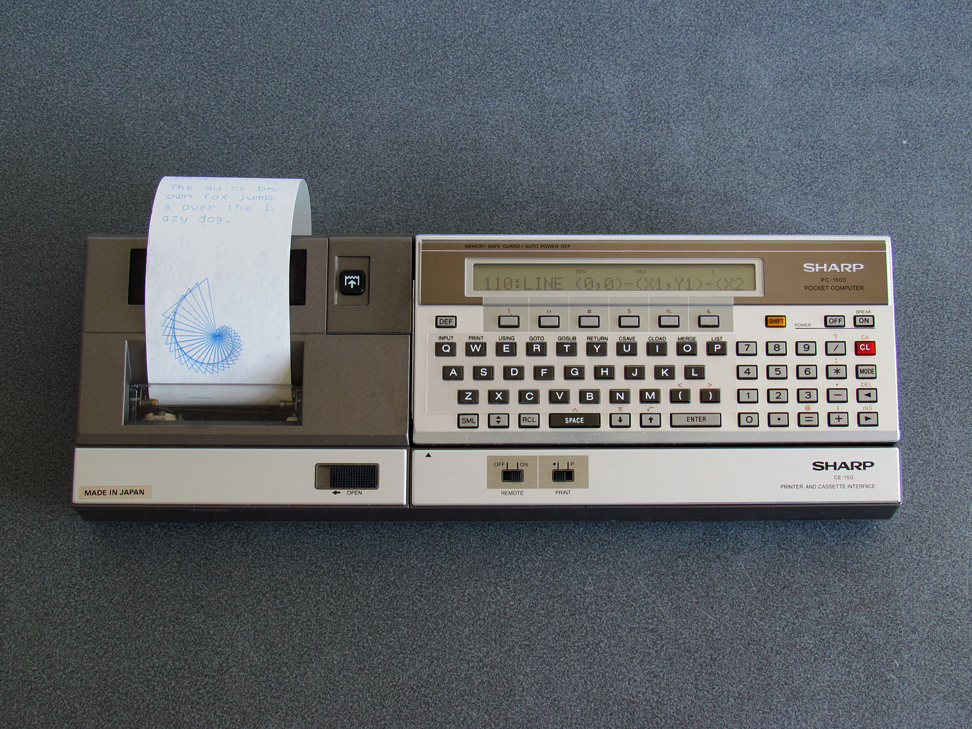
Sharp PC-1500 Pocket Computer connected to the CE-150 Printer and Cassette Interface
The Sharp PC-1500 is a small computer from the early 1980s that can run programs primarily written in BASIC. Programs can be saved to and loaded back from cassette tape but to do this requires it to be connected to the CE-150, a cassette interface that also includes a four-colour plotter. It's the plotter that really attracted me to the computer in the first place, but being able to load programs from cassette rather than having to type them in by hand is definitely a very handy feature!
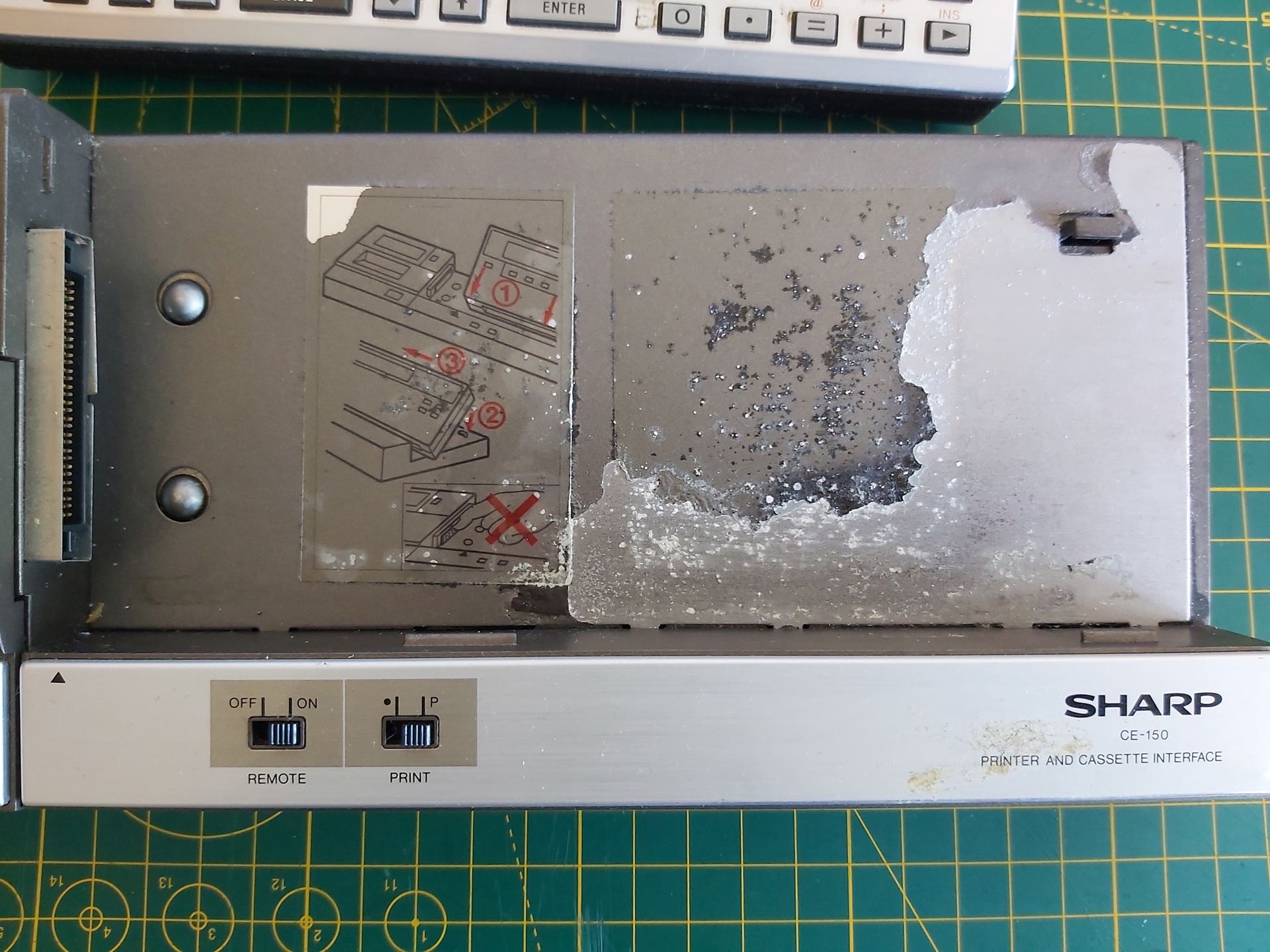
Unfortunately this CE-150 interface contains an internal battery pack of five Ni-Cd cells. A certain amount of battery leakage is a risk in any old piece of electronics hardware, but having said battery pack soldered directly in with no easy way for the user to remove it for long-term storage makes it more of a certainty than a risk. My CE-150 had not escaped, with heavy corrosion visible on the metal plate under the computer…
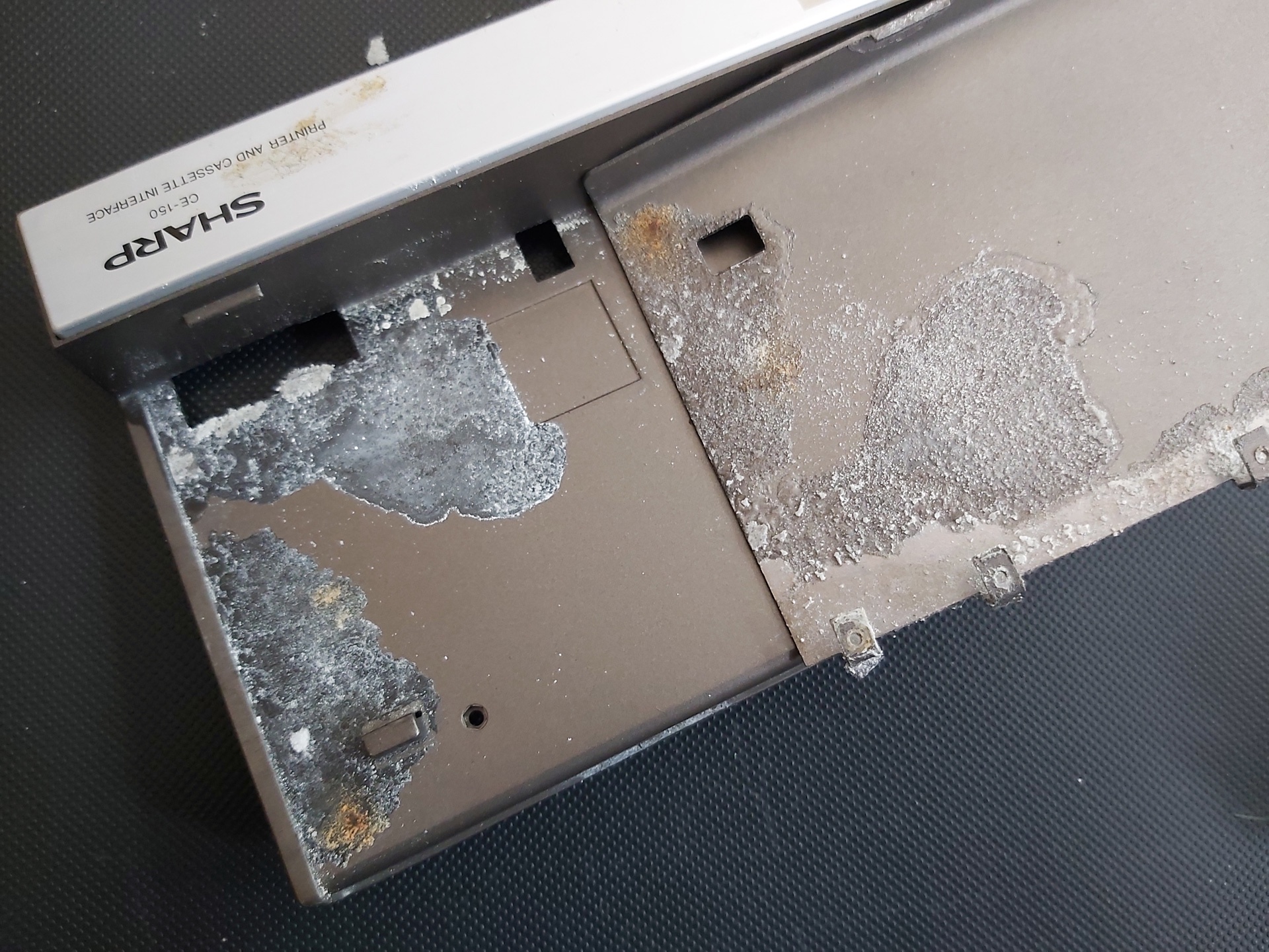
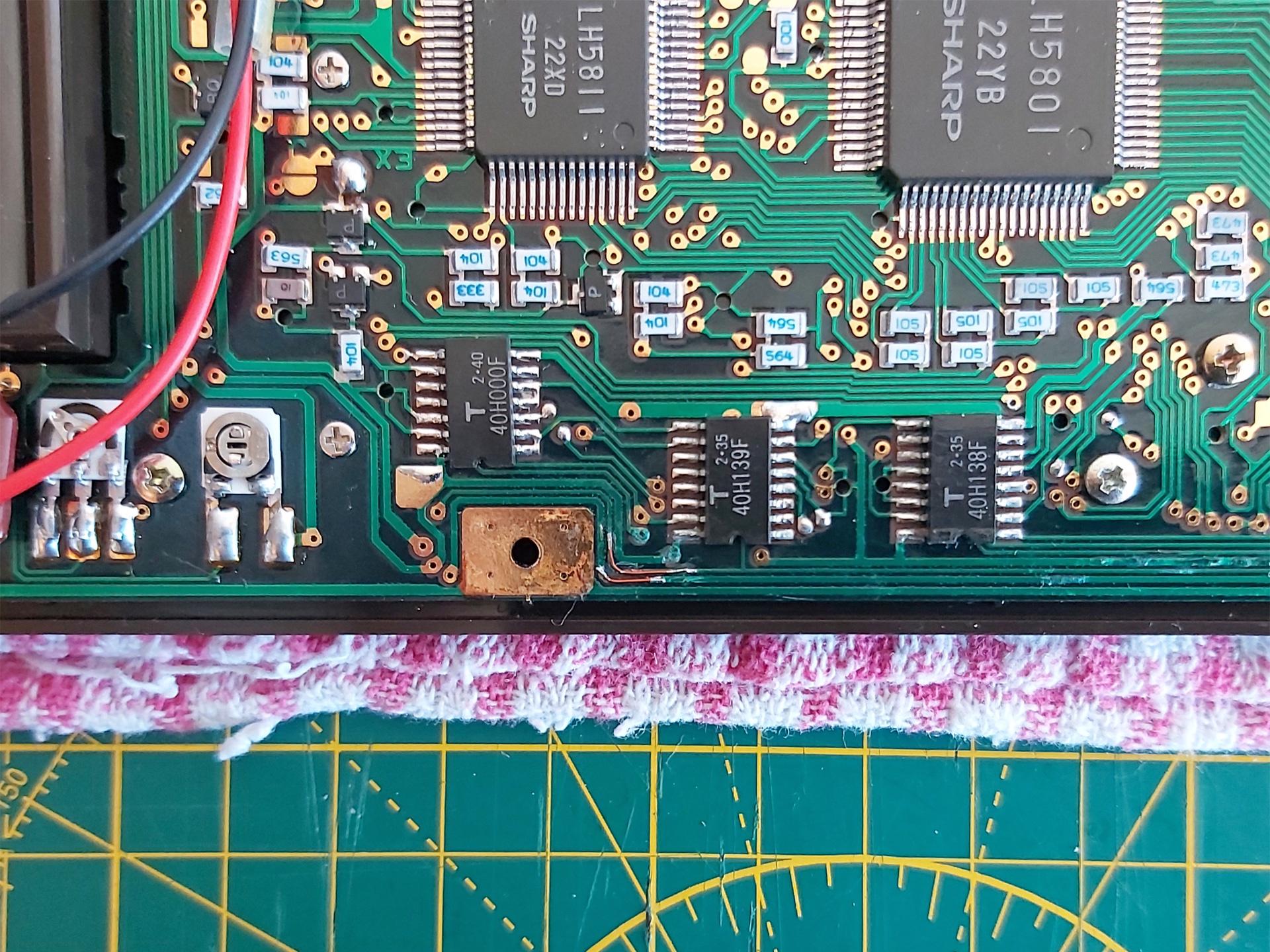
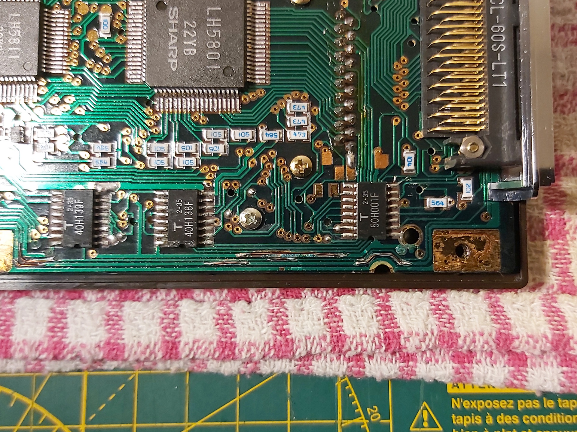
The inside of the PC-1500 was a bit better and not quite as musty-smelling, but circuit board traces had definitely been eaten away in places and some of the internal metal structure was looking a bit crusty.
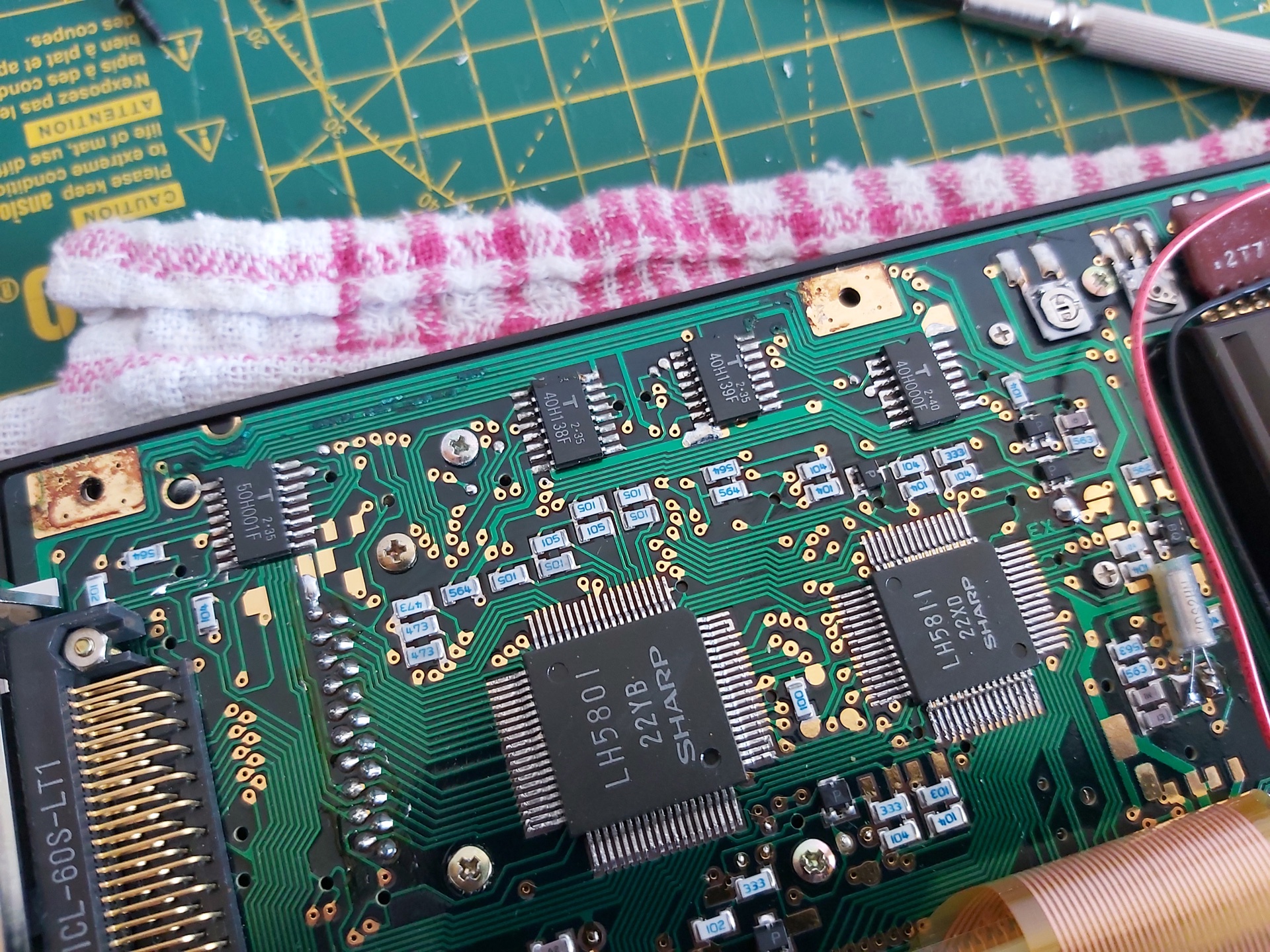
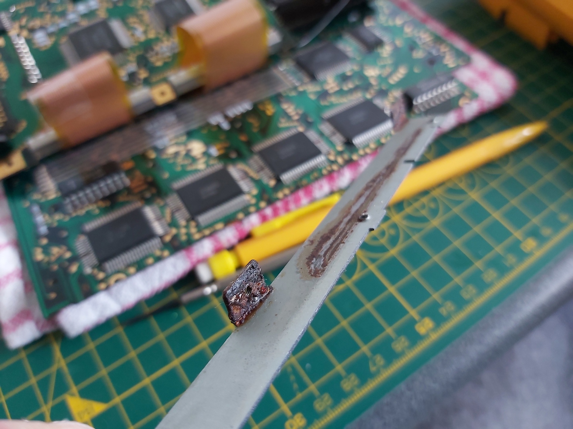
I cleaned up the rusty metal using some appliance descaler (and recorded a video of the process, which can be found on YouTube) then got to work with a scalpel and some fine enamelled copper wire to repair the damaged traces.
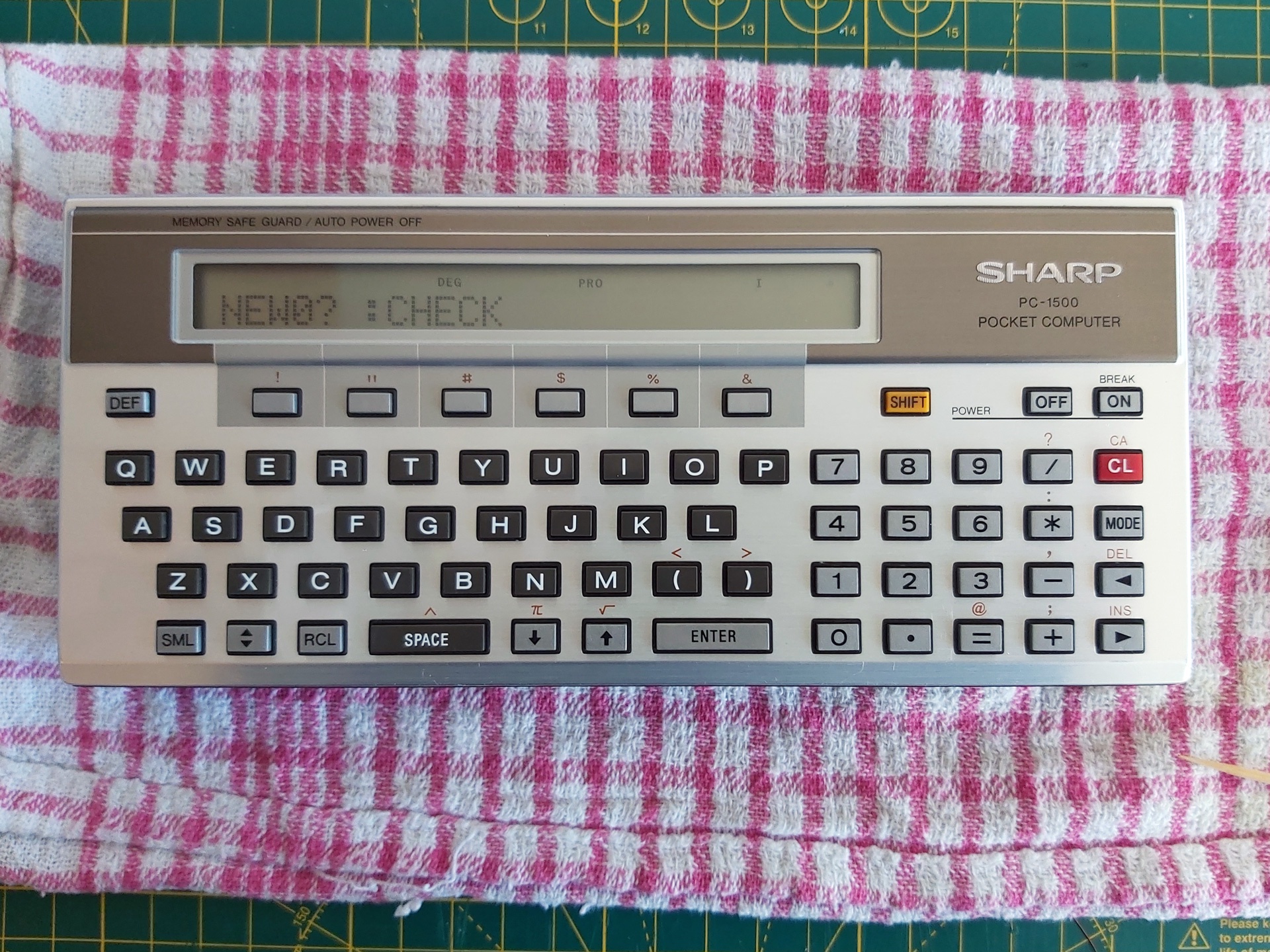
Thankfully when I put it all back together again I was greeted by the NEW0? :CHECK prompt, so I connected the computer to the CE-150 and confirmed I could save and load back programs using my PC in place of a cassette recorder. Hooray!
When looking to see what other people had managed to achieve with the computer I found the Sharp PC-1500 (TRS-80 PC-2) resource page which hosts several games and applications which can be downloaded in WAV format. I downloaded a few, but when playing them back on my PC the PC-1500 would refuse to load them. It could load from my own recordings, why not these?
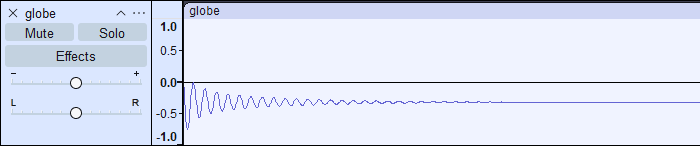
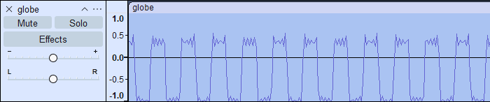
The odd thing is that my own recordings started with a few seconds of constant pilot tone followed by the varying pulses of the program data I was trying to load. When playing back the downloaded recordings they'd start with silence and only make sound when they got to the actual data – and that data sounded quite unlike what my own recordings sounded like. What was going on? I opened a recording in Audacity to see what it looked like, and zoomed in:
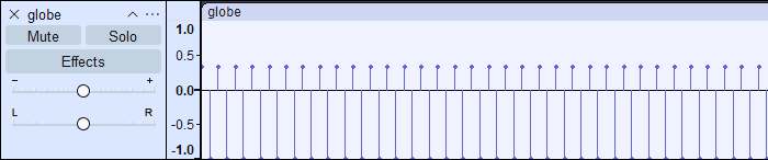
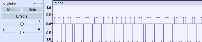
That looks like the pilot tone, in that it alternates between high and low at a fixed frequency, though it's only one sample high then one sample low so is a square wave rather than the smooth sine wave I was expecting. The cassette format uses frequency-shift keying so I would expect to see data further on in the recording at half the frequency, or twice the period, i.e. two samples high and then two samples low. Scrolling along, I certainly find that:
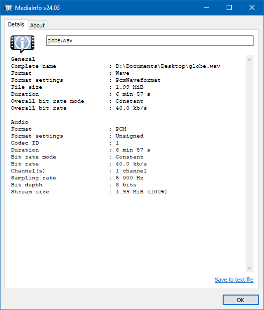
Why does it look so spiky, though? It would only need to look like that if it had been sampled at an extremely low rate, and indeed that's what I found – these files are recorded at a 5kHz sample rate:
5kHz is a pretty unusual (and very low!) sample rate that I suspected my sound card was not handling particularly gracefully. Typically audio would need to be resampled to 44.1kHz or 48kHz before playing back, so I thought I'd try resampling in Audacity. This produced this weirdness:
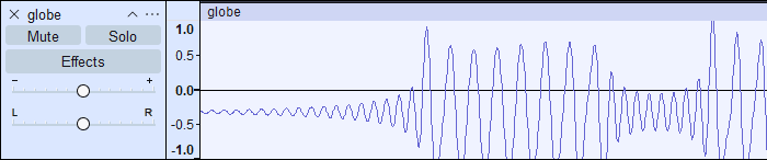
Instead of a sine wave that alternates between two frequencies, I ended up with something more akin to an amplitude-modulated signal! The high-frequency pilot also disappears entirely, apart from what looks to be some initial ringing:
Now, this is a complete guess, but I suspect that what is happening is an attempt to reduce unpleasant harmonics in the resampled audio. A square wave (such as the one we're resampling) produces a lot of harmonics at higher frequencies. As the original audio was sampled at 5kHz, the highest frequency that this could represent was 2.5kHz (alternating high and low each sample, as per the pilot tone). A low-pass filter at 2.5kHz could therefore reduce the harmonics, though I'd still expect some of it to get through (rather than it being apparently being attenuated to zero in this case!) In any case, the signal is being destroyed by the resampling process, so it's no wonder the computer can't load the data.
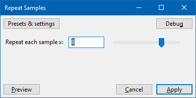
So, what's the solution? A simpler resampling algorithm that just duplicates samples (a sort of "nearest neighbour") should give us an acceptable square wave when processing, however I could not find any way to achieve this natively in Audacity. Fortunately, though, there's a Nyquist Plugin script that can be used to repeat all samples (install via Tools→Nyquish Plugin Installer, then check it's listed in Tools→Plugin Manager – it will appear as Effect→Repeat Samples). As we want to end up around 44.1kHz the plugin can be used to repeat each sample eight times, which would take our 5kHz sample rate to 40kHz:
↓
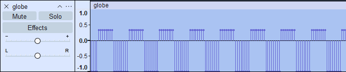
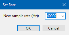
When played back the pilot tone can finally be heard, but it's at much too low a pitch! This is because the samples have been repeated eight times, but the track's sample rate hasn't been increased to match. This can be done by right-clicking the track and selecting Rate→Other and entering 40kHz:
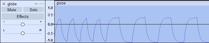
Now when the clip is played back it sounds as it should. As a further experiment, the sample rate could be changed from its somewhat odd 40kHz to a more conventional 44.1kHz via Tracks→Resample. When this is done, the nice clean square wave loses definition again:
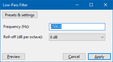
As I mentioned earlier, square waves have a lot of harmonics, and the resampling process makes these harmonics extremely visible riding on top and bottom of each cycle of the square wave. There is one way to clean this up quite nicely, however – as we want to cull high-frequency harmonics, and as the original recording could only represent frequencies up to 2.5kHz we can apply a low-pass filter at 2.5kHz from the Effects menu:
↓
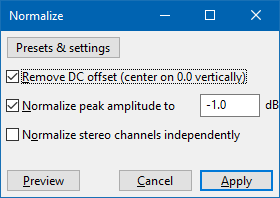
This resulting file sounds much better and loads into the computer as it should. It's a bit of a convoluted process, but it does at least bypass the resampling weirdness that distorts the original files in such a way that they can't be loaded. The only additional step I might recommend is to more neatly balance the signal around zero by normalising it as the first step:
In summary, the steps are as follows:
- Normalise the file (Effect→Normalize)
- Repeat all samples by 8× (Effect→Repeat Samples)
- Set track sample rate to 8× what it was (right-click, Rate→Other, multiply the value by 8)
- Resample to 44.1kHz (Tracks→Resample)
- Low-pass filter at 2.5kHz (Effect→Low-Pass Filter)
Happy tape loading!
1-Wire interfacing with the Cambridge Z88
Sunday, 17th December 2023
I've been having a tricky time buying LM35DZ analogue temperature sensors for a project recently. One pair of probes and a bag of loose components labelled LM35DZ turned out to be regular NPN transistors with a fake label on them, and another pair of probes ended up being DS18B20 digital temperature sensors.
Whilst the DS18B20 temperature sensors were useless for the project I had in mind they were still functioning components. These use the 1-Wire serial bus, a bus named for the way that its single data line can also be used to parasitically power the devices on the bus. Electrically the bus is open drain with a pull-up resistor that idles in the high state which any device can drive low. The master initiates all communication and you can have multiple peripheral devices connected to the bus in an arrangement called a MicroLAN.
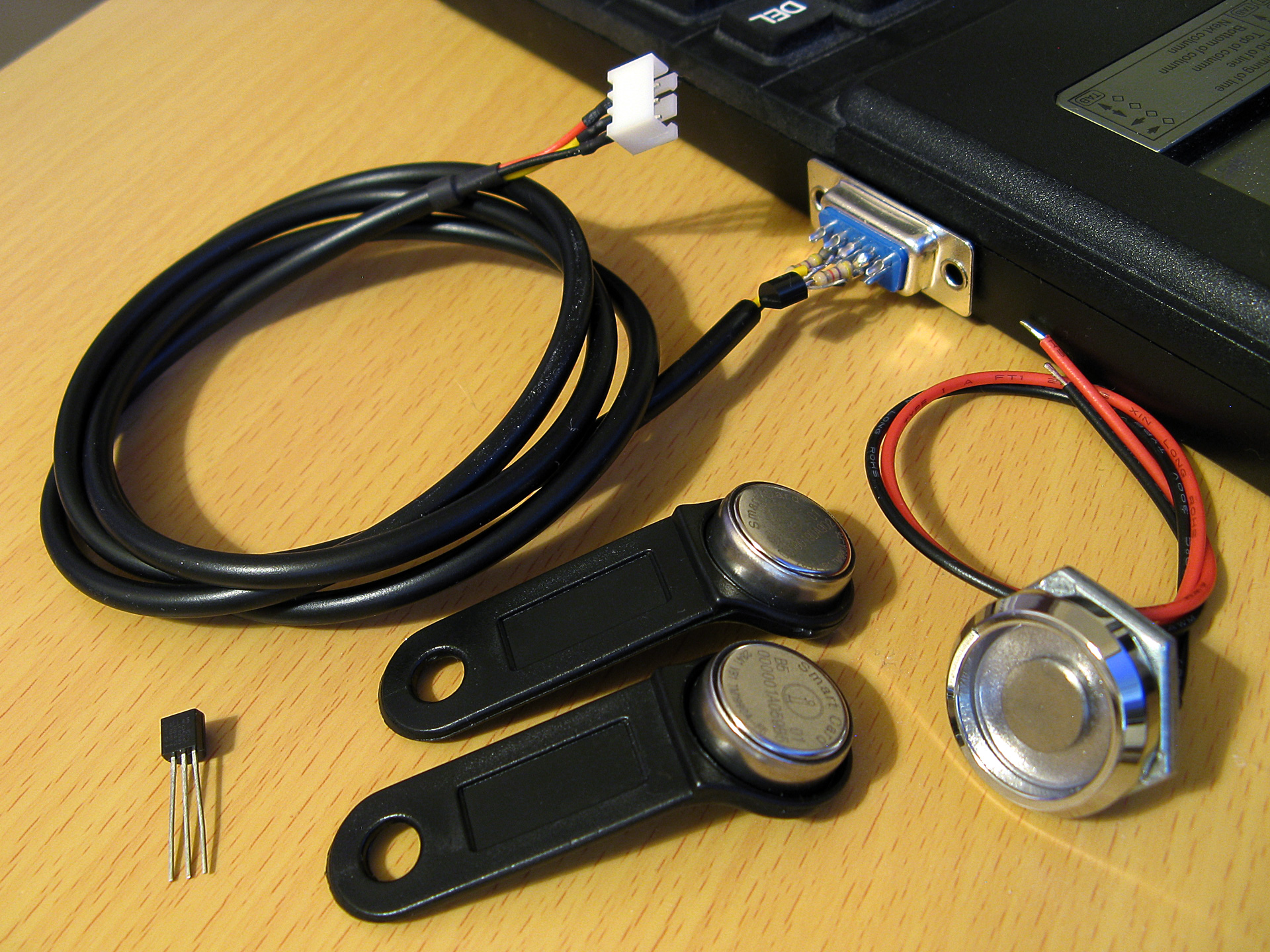
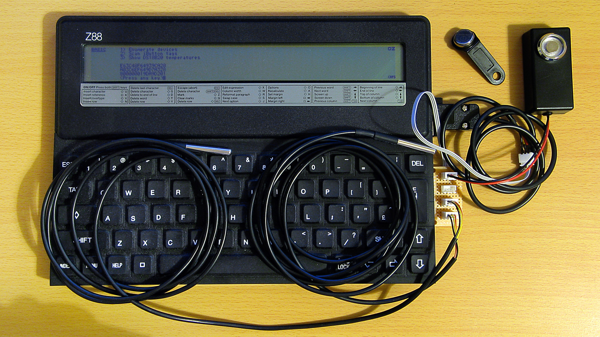
A selection of 1-Wire devices and a 1-Wire interface adaptor plugged into a Z88 computer
I'd had some limited experience working with the 1-Wire bus as part of my version of the Superprobe but now that I had a collection of temperature sensors I thought it might be worth revisiting, this time on the Cambridge Z88.
1-Wire adaptor for the Z88 serial port
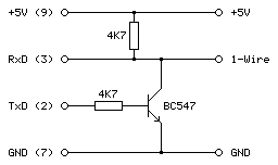
To connect 1-Wire devices to the Z88 some sort of adaptor is required and one that plugged into the computer's serial port seemed like a sensible enough option. The Z88's serial port hardware normally handles all the communications for you however it is possible to directly control the logic levels of the serial port's output pins and read back the status of the input pins via some hardware registers.
The TXD line can be +5V for a logic 0 and -6V for a logic 1, adhering to the RS-232 standard. When idle TXD is in its logic 1 state, outputting -6V. Bit ITX (3) in the TXC (&E4) register can be used to invert the behaviour of the TXD pin, so by setting this bit we can change the state of the pin from -6V to +5V.
As we need to have an open-drain bus we can use an NPN transistor with the base connected to the TXD line via a current-limiting resistor, the emitter connected to ground and the collector driving the 1-Wire bus. By default the TXD pin will output -6V, the transistor will be switched off and the bus will be pulled high. When the TXD pin state is inverted it will output +5V, the transistor will switch on and drive the line low.
The state of the RXD line can be read directly via bit RXD (4) in the RXE (&E1) register. The lines appear to be weakly held to 0V and read back a 0 bit in this state, flipping to a 1 bit when the voltage rises above around 2V. In this case we can connect the 1-Wire bus directly to the RXD input and be able to read back the current state.
The circuit for the adaptor, including the 4.7K pull-up resistor, appears as follows:
This can be tested in a BASIC program. To determine the input state we can read from the RXE port register (&E1) and check the state of the RXD bit (4):
10 RXE=&E1:M_RXERXD=&10
20 REPEAT
30   PRINT ~(GET(RXE) AND M_RXERXD)
40 UNTIL FALSE
The mask value M_RXERXD is specified as 24=&10 to correspond to the bit four. When run this program displays &10 in hex (showing bit 4 is set and the bus level is therefore high) until the 1-Wire bus line is connected to ground, when the value changes to 0 (showing bit 4 is reset and the bus level is therefore low).
To change the output state we need to write to bit ITX (3) of the TXC register (&E4). However, when writing to the hardware port we only want to change that bit and leave the others alone. The TXC register is a write-only port, so we can't retrieve its previous state by reading from the port. Fortunately the OS maintains a copy of the last value written as a "soft copy" in RAM at address &04E4 and this can be read with the ? indirection operator:
10 TXC=&E4:M_TXCITX=&08
20 SC=&400
30 TXC_OLD=SC?TXC
40 PUT TXC,TXC_OLD OR M_TXCITX
50 IF INKEY(100)
60 PUT TXC,TXC_OLD
The above program reads the old state of the TXC port from the soft copy, ORs it with the mask of the ITX bit (23=&08) and then outputs that to the TXC port. This has the effect of inverting the TXD line, driving the 1-Wire bus low. The program then waits one second with a dummy keyboard read before restoring the old value of the TXC port to release the 1-Wire bus.
Normally if changing the state of the serial port it would be good manners to update the soft copy of the serial port state however as the program is just going to be sending short low pulses before returning the port to its previous state this step is omitted.
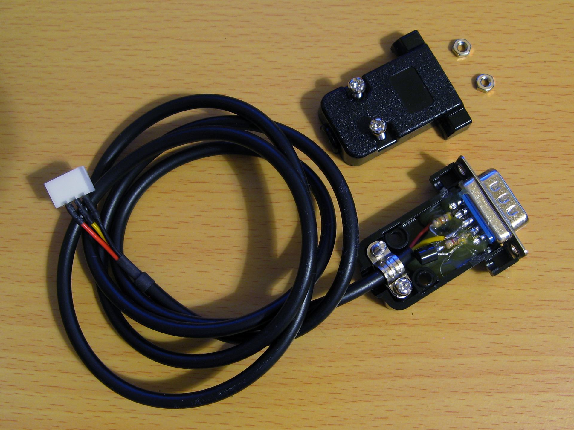
After testing that the circuit worked on a breadboard a more permanent version was assembled in a DE-9 shell as above. As the clips that hold in the DE-9 connector had to cut off to allow it to fit in the Z88's recessed port the circuit ended up being secured with copious amounts of hot glue, which is far from ideal, but nobody will see when it's all screwed back together.
Bit-level protocol
Now that we can electrically control the bus we need to know how to transfer data on it. This is done by timed pulses, where the bus master will hold the bus line low for a certain amount of time, release it, then check to see if any devices on the bus are holding it low in return. This is summarised in the following timing diagram from Microchip's AN1199, 1-Wire Communication with PIC Microcontroller:
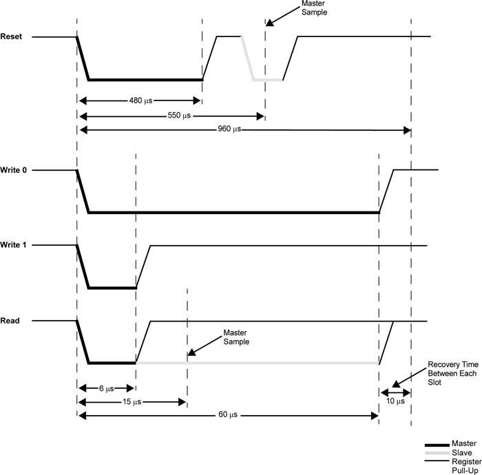
The first thing that needs to be done is to reset all devices on the bus. This is done by holding the bus low for 480μs then releasing it for at least 480μs. If any peripheral devices are present on the bus they will drive the line low after the low pulse from the master, so the full reset procedure is as follows:
- Master drives bus low
- Delay 480μs
- Master releases bus high
- Delay 70μs
- Sample bus state: if high, no peripheral devices present, if low at least one device present.
- Delay 410μs
Once reset, data can be transmitted from the master to peripheral devices bit-by-bit in a similar fashion to the reset pulse, albeit with different timing.
To send a 0 bit:
- Master drives bus low
- Delay 60μs
- Master releases bus high
- Delay 10μs
To send a 1 bit:
- Master drives bus low
- Delay 6μs
- Master releases bus high
- Delay 64μs
Bytes are transferred as eight individual bits, least-significant bit first. The protocol is also tolerant of large delays between individual bits.
Once data has been sent to a peripheral, it may respond with data of its own. The master is still in control of clocking the data out of the peripheral, and the process is as follows:
- Master drives bus low
- Delay 6μs
- Master releases bus high
- Delay 9μs
- Sample bus state to read data bit from peripheral
- Delay 55μs
The overall timing for reading a bit is the same as the timing for sending a 1 bit (an initial 6μs low pulse from the master and a total bit time of 70μs) so in practice only one routine needs to be implemented and the value returned from the bus during read operations can be ignored during write operations.
Software choice for the Z88
I thought it would be nice to be able to interact with 1-Wire devices from a BASIC program. BBC BASIC on the Z88 does provide direct access to the hardware and would make controlling the 1-Wire bus line possible, as demonstrated earlier, however I don't think it would provide the timing accuracy required to produce the appropriate pulses from the master. Fortunately it does include a Z80 assembler and so a mixture of a BASIC program that provides the high-level routines and assembly snippets for the low-level 1-Wire protocol implementation seemed like an appropriate mix of languages.
When you CALL an assembly routine from BASIC the Z80's registers are initialised to the values of the corresponding static variables, for example A is set to A%, H to H%, L to L% etc. You can't return a value directly – for that you'd need USR – however it's a bit easier to just store the return value in memory and retrieve that from BASIC after the CALL returns.
A rough starting point for the 1-Wire program is as follows:
 10 REM 1-WIRE DEMO
 20 PROC_1W_INIT
 30 PRINT FN_1W_RESET
 40 END
 50 :
 60 REM 1-WIRE ROUTINES
 70 END
 80 DEFPROC_1W_INIT
 90 ow_code_size=256:DIM ow_code ow_code_size-1
100 RXE=&E1:M_RXERXD=&10
110 TXC=&E4:M_TXCITX=&08
120 SC=&400
130 FOR opt=0 TO 2 STEP 2
140   P%=ow_code
150   [OPT opt
160   .ow_buf DEFB 0 \ temporary transfer buffer
170   :
180   .ow_reset
190   IN A,(RXE):AND M_RXERXD:CP M_RXERXD:SBC A,A:LD (ow_buf),A:RET NZ \ check bus is idle
200   DI:LD A,(SC+TXC):OR M_TXCITX:OUT (TXC),A \ hold bus low
210   LD B,120:DJNZ P% \ delay
220   AND NOT M_TXCITX:OUT (TXC),A \ release bus
230   LD B,18:DJNZ P% \ delay
240   IN A,(RXE):AND M_RXERXD:CP M_RXERXD:CCF:SBC A,A:LD (ow_buf),A \ sample presence
250   LD B,100:DJNZ P% \ delay
260   EI:RET
270   :
280   ]
290 NEXT
300 ENDPROC
310 :
320 REM Resets bus, retuns TRUE if any devices are present
330 DEFFN_1W_RESET:CALL ow_reset:=?ow_buf=0
The first few lines are going to be where our BASIC program is. This calls the procedure PROC_1W_INIT which will set things up by assembling any required Z80 code. It then calls FN_1W_RESET which is a function that resets the 1-Wire bus and checks to see if any devices assert their presence.
PROC_1W_INIT starts by allocating some memory for the assembled code to live, defines some constants for the IO ports and then runs through the two passes of the assembly process in a loop. Within the assembly block is a variable (ow_buf) which will be used to store data due to be returned by the assembly routines. The ow_reset assembly routine then follows – this first checks to see if the bus is idle (floating high) and if so it disables interrupts, holds the bus low for 480μs, releases the bus and waits 70μs, samples the state of the bus to check for device presence (storing the result in ow_buf), then delays another 410μs.
The delay loops are simple DJNZ loops with B corresponding to the length of the delay and the timings were roughly calculated first based on the number of cycles each loop would take and the Z88's 3.2768MHz CPU clock speed. They were then adjusted slightly using a logic analyser to ensure the timing was as close as could be managed to the 1-Wire protocol's specifications.
The ow_reset routine has been written so that following a successful presence check ow_buf should contain 0, and if there is a problem it will contain a non-zero value. This is used by the FN_1W_RESET wrapper function which just calls ow_reset and returns TRUE if ow_buf is zero afterwards.
If you run the program you should see that the program will display 0 (FALSE) on the screen until a 1-Wire device is connected to the adaptor, at which point it will display -1 (TRUE) instead to indicate the device's presence. This isn't a very useful program, but shows how BASIC and assembly will be mixed to build the rest of the 1-Wire routines.
Sending and receiving bits and bytes
Now that we know a device is present on the bus after a reset we need to be able to send and receive bits and bytes. Sending a 0 bit is a bit simpler than resetting, as we don't need to check for any response – just hold the line low for 60μs then release it back high for 10μs. This can be implemented as follows:
.ow_put_0
DI
LD A,(SC+TXC):OR M_TXCITX:OUT (TXC),A \ hold bus low
LD B,15:DJNZ P% \ delay
AND NOT M_TXCITX:OUT (TXC),A \ release bus
NOP \ delay
EI:RET
Sending a 1 bit has the same overall timing as reading a bit, so instead of writing separate routines to send a 1 bit and read a bit just one routine is required that handles both situations:
.ow_put_1
DI
LD A,(SC+TXC):OR M_TXCITX:OUT (TXC),A \ hold bus low
NOP \ delay
AND NOT M_TXCITX:OUT (TXC),A \ release bus
PUSH HL:POP HL \ delay
IN A,(RXE):AND M_RXERXD:SUB M_RXERXD:CCF \ sample bit
LD A,(ow_buf):RRA:LD (ow_buf),A \ store bit
LD B,7:DJNZ P% \ delay
EI:RET
This holds the bus low for 6μs, releases it and waits 9μs, samples a bit from the bus and rotates it into the ow_buf transfer buffer, then waits 55μs.
These routines could be wrapped up for use in BASIC but it's not too useful to be able to send or receive single bits, normally we'd need to transfer whole 8-bit bytes. The ow_put_1 routine already handles updating the ow_buf with each received bit, so a byte receiving routine can be put together by just calling ow_put_1 eight times in a loop:
.ow_get_byte
LD B,8 \ 8 bits to receive
.ow_get_loop
PUSH BC:CALL ow_put_1:POP BC \ receive single bit
DJNZ ow_get_loop \ loop
LD A,(ow_buf):RET \ store
A send routine can be put together with a similar loop that shifts out the bit to send and then calls either the ow_put_0 or ow_put_1 routine depending on whether it's a 0 or 1 bit that's required. Bits will usually be shifted out into the carry register, so a new ow_put_carry routine that sends the bit stored in the carry flag makes this a bit easier, e.g.
.ow_put_carry
JR C,ow_put_1
JR ow_put_0
...which will be called by the ow_put_byte routine, as follows:
.ow_put_byte
LD C,A:LD B,8 \ value to send in C, send 8 bits
.ow_put_loop
SRL C:PUSH BC:CALL ow_put_carry:POP BC \ shift and send single bit
DJNZ ow_put_loop \ loop
RET
It is also quite useful to be able to send or receive blocks of data at once – for example, sending or receiving the 64-bit device IDs requires sending or receiving 8 bytes of data at a time. To complement ow_get_byte and ow_put_byte we can write ow_get_bytes and ow_put_bytes routines to send or receive the block of data addressed by HL, length BC:
.ow_get_bytes
LD A,B:OR C:RET Z:DEC BC \ have we finished?
PUSH BC:CALL ow_get_byte:POP BC \ get a byte
LD (HL),A:INC HL:JR ow_get_bytes \ store and loop
:
.ow_put_bytes
LD A,B:OR C:RET Z:DEC BC \ have we finished?
LD A,(HL):INC HL \ fetch
PUSH BC:CALL ow_put_byte:POP BC:JR ow_put_bytes \ send and loop
All of these can now be wrapped up as procedures or functions so they can be more easily used from a BASIC program:
REM Transmits a single byte
DEFPROC_1W_PUT(A%)CALL ow_put_byte:ENDPROC
REM Transmits a block of bytes
DEFPROC_1W_PUTS(L%,C%)LOCAL H%,B%:H%=L%DIV256:B%=C%DIV256:CALL ow_put_bytes:ENDPROC
REM Receives a single byte
DEFFN_1W_GET:CALL ow_get_byte:=?ow_buf
REM Receives a block of bytes
DEFPROC_1W_GETS(L%,C%)LOCAL H%,B%:H%=L%DIV256:B%=C%DIV256:CALL ow_get_bytes:ENDPROC
BASIC's integer variables are 32-bit integers so when passing the 16-bit address or length parameters the target register is the least-significant one (L for HL, C for BC) and the most-significant register (H or B) is populated by dividing the value by 256.
This can all be put together in the following demonstration program. It initialises the routines, resets the bus and checks for presence, then sends the "read ROM" command &33 which will make any connected devices respond with their ROM ID. It then reads back the eight bytes corresponding to the device ID then prints them back in hexadecimal.
 10 DIM ID 7:REM Storage for device ID
 20 PROC_1W_INIT
 30 IF FN_1W_RESET=FALSE PRINT "No devices found.":END
 40 PROC_1W_PUT(&33):REM "Read ROM" command
 50 PROC_1W_GETS(ID,8):REM Read eight bytes of device ID
 60 FOR I=7 TO 0 STEP -1:PRINT ~ID?I;:NEXT:PRINT:REM Print device ID bytes
 70 END
 80 :
 90 REM 1-WIRE ROUTINES
100 END
110 DEFPROC_1W_INIT
120 ow_code_size=256:DIM ow_code ow_code_size-1
130 RXE=&E1:M_RXERXD=&10
140 TXC=&E4:M_TXCITX=&08
150 SC=&400
160 FOR opt=0 TO 2 STEP 2
170   P%=ow_code
180   [OPT opt
190   .ow_buf DEFB 0 \ temporary transfer buffer
200   :
210   .ow_reset
220   IN A,(RXE):AND M_RXERXD:CP M_RXERXD:SBC A,A:LD (ow_buf),A:RET NZ \ check bus is idle
230   DI:LD A,(SC+TXC):OR M_TXCITX:OUT (TXC),A \ hold bus low
240   LD B,120:DJNZ P% \ delay
250   AND NOT M_TXCITX:OUT (TXC),A \ release bus
260   LD B,18:DJNZ P% \ delay
270   IN A,(RXE):AND M_RXERXD:CP M_RXERXD:CCF:SBC A,A:LD (ow_buf),A \ sample presence
280   LD B,100:DJNZ P% \ delay
290   EI:RET
300   :
310   .ow_put_carry
320   JR C,ow_put_1 \ fall-through
330   :
340   .ow_put_0
350   DI
360   LD A,(SC+TXC):OR M_TXCITX:OUT (TXC),A \ hold bus low
370   LD B,15:DJNZ P% \ delay
380   AND NOT M_TXCITX:OUT (TXC),A \ release bus
390   NOP \ delay
400   EI:RET
410   :
420   .ow_put_1
430   DI
440   LD A,(SC+TXC):OR M_TXCITX:OUT (TXC),A \ hold bus low
450   NOP \ delay
460   AND NOT M_TXCITX:OUT (TXC),A \ release bus
470   PUSH HL:POP HL \ delay
480   IN A,(RXE):AND M_RXERXD:SUB M_RXERXD:CCF \ sample bit
490   LD A,(ow_buf):RRA:LD (ow_buf),A \ store bit
500   LD B,7:DJNZ P% \ delay
510   EI:RET
520   :
530   .ow_put_byte
540   LD C,A:LD B,8 \ value to send in C, send 8 bits
550   .ow_put_loop
560   SRL C:PUSH BC:CALL ow_put_carry:POP BC \ shift and send single bit
570   DJNZ ow_put_loop \ loop
580   RET
590   :
600   .ow_put_bytes
610   LD A,B:OR C:RET Z:DEC BC \ have we finished?
620   LD A,(HL):INC HL \ fetch
630   PUSH BC:CALL ow_put_byte:POP BC:JR ow_put_bytes \ send and loop
640   :
650   .ow_get_byte
660   LD B,8 \ 8 bits to receive
670   .ow_get_loop
680   PUSH BC:CALL ow_put_1:POP BC \ receive single bit
690   DJNZ ow_get_loop \ loop
700   LD A,(ow_buf):RET \ store
710   :
720   .ow_get_bytes
730   LD A,B:OR C:RET Z:DEC BC \ have we finished?
740   PUSH BC:CALL ow_get_byte:POP BC \ get a byte
750   LD (HL),A:INC HL:JR ow_get_bytes \ store and loop
760   :
770   ]
780 NEXT
790 IF P%-ow_code>ow_code_size PRINT"Code size: "P%-ow_code:END
800 ENDPROC
810 :
820 REM Resets bus, retuns TRUE if any devices are present
830 DEFFN_1W_RESET:CALL ow_reset:=?ow_buf=0
840 REM Transmits a single byte
850 DEFPROC_1W_PUT(A%)CALL ow_put_byte:ENDPROC
860 REM Transmits a block of bytes
870 DEFPROC_1W_PUTS(L%,C%)LOCAL H%,B%:H%=L%DIV256:B%=C%DIV256:CALL ow_put_bytes:ENDPROC
880 REM Receives a single byte
890 DEFFN_1W_GET:CALL ow_get_byte:=?ow_buf
900 REM Receives a block of bytes
910 DEFPROC_1W_GETS(L%,C%)LOCAL H%,B%:H%=L%DIV256:B%=C%DIV256:CALL ow_get_bytes:ENDPROC
When connected to an iButton fob the program prints
55 0 0 1 A0 1A 57 1
...which matches the ID printed on it.
An example of a TM1990A iButton fob (middle) along with the probe used to read it (top)
When connected to a DS18B20 temperature sensor the program prints
B9 0 0 1 D1 97 5D 28
The least significant byte of the 64-bit ID is the family code – &01 for the iButton fob indicates it's a "silicon serial number" type device and &28 for the DS18B20 indicates it's a "programmable resolution digital thermometer".
The 1-Wire bus supports multiple peripheral devices connected to a single master. If we try that we still get something that looks like an ID back:
11 0 0 1 80 12 55 0
This happens because it's an open-drain bus and any device holding the line low will take priority over any device releasing the line high. In effect the data read back is ANDed together, so the most-significant byte received is &55 AND &B9 which gives us the &11 we see. Fortunately that most-significant byte does give us a good opportunity to detect such invalid data!
Error detection with a CRC
Some data payloads include a CRC value. The most-significant byte of a 64-bit device ID is such a CRC, with the least-significant byte being the family code. The exact details for the CRC calculation can be found in the article Understanding and Using Cyclic Redundancy Checks with Maxim 1-Wire and iButton Products however for our purposes a Z80 implementation can be written as follows:
.ow_crc
LD B,8:LD DE,(ow_buf):LD D,A \ E = accumulated CRC, D = value to add
.ow_crc_loop
LD A,E:XOR D:SRL D:SRL A:JR C,ow_crc_odd \ XOR and shift bits
SRL E:DJNZ ow_crc_loop:LD A,E:LD (ow_buf),A:RET \ even CRC value
.ow_crc_odd:SRL E:LD A,&8C:XOR E:LD E,A:DJNZ ow_crc_loop:LD (ow_buf),A:RET \ odd CRC value
:
.ow_crc_block
XOR A:LD (ow_buf),A \ reset CRC
.ow_crc_block_loop
LD A,B:OR C:LD A,(ow_buf):RET Z:DEC BC \ have we finished?
LD A,(HL):INC HL:PUSH BC:CALL ow_crc:POP BC:JR ow_crc_block_loop \ update CRC
ow_crc updates the current calculated CRC value (stored in ow_buf) with the next data byte from the accumulator. ow_crc_block calculates the CRC for a block of data pointed to by HL, length BC, using the ow_crc routine. A couple of BASIC functions can then be written, one to calculate the CRC of a block of data and another to check that the last byte of the block corresponds to the CRC of the preceding data:
REM Calculates the CRC of a block of data
DEFFN_1W_CRC(L%,C%)LOCAL H%,B%:H%=L% DIV256:B%=C%DIV256:CALL ow_crc_block:=?ow_buf
REM Checks if a CRC at the end of a block of data matches
DEFFN_1W_CRC_CHECK(L%,C%)=FN_1W_CRC(L%,C%)=(L%?C%)
These two can now be used to check that a device ID is valid. The CRC is also appended to other data reports, such as reading the scratchpad memory of a temperature sensor, so it's a useful routine to have. A new program which checks the CRC is as follows:
 10 DIM ID 7
 20 PROC_1W_INIT
 30 REPEAT
 40   REPEAT UNTIL FN_1W_RESET:REM Wait for device to be present
 50   PROC_1W_PUT(&33):REM Read ROM
 60   PROC_1W_GETS(ID,8):REM Fetch ID
 70   IF FN_1W_CRC_CHECK(ID,7) VDU 7:PRINT "Detected ";FN_1W_ID$(ID);" at ";TIME$:REM Print if valid
 80   REPEAT UNTIL FN_1W_RESET=FALSE:REM Wait for device to be disconnected
 90 UNTIL FALSE
100 END
110 :
120 REM 1-WIRE ROUTINES
130 END
140 DEFPROC_1W_INIT
150 ow_code_size=256:DIM ow_code ow_code_size-1
160 RXE=&E1:M_RXERXD=&10
170 TXC=&E4:M_TXCITX=&08
180 SC=&400
190 FOR opt=0 TO 2 STEP 2
200   P%=ow_code
210   [OPT opt
220   .ow_buf DEFB 0 \ temporary transfer buffer
230   .ow_conf DEFB 0 \ stores last bit conflict index
240   :
250   .ow_reset
260   IN A,(RXE):AND M_RXERXD:CP M_RXERXD:SBC A,A:LD (ow_buf),A:RET NZ \ check bus is idle
270   DI:LD A,(SC+TXC):OR M_TXCITX:OUT (TXC),A \ hold bus low
280   LD B,120:DJNZ P% \ delay
290   AND NOT M_TXCITX:OUT (TXC),A \ release bus
300   LD B,18:DJNZ P% \ delay
310   IN A,(RXE):AND M_RXERXD:CP M_RXERXD:CCF:SBC A,A:LD (ow_buf),A \ sample presence
320   LD B,100:DJNZ P% \ delay
330   EI:RET
340   :
350   .ow_put_carry
360   JR C,ow_put_1 \ fall-through
370   :
380   .ow_put_0
390   DI
400   LD A,(SC+TXC):OR M_TXCITX:OUT (TXC),A \ hold bus low
410   LD B,15:DJNZ P% \ delay
420   AND NOT M_TXCITX:OUT (TXC),A \ release bus
430   NOP \ delay
440   EI:RET
450   :
460   .ow_put_1
470   DI
480   LD A,(SC+TXC):OR M_TXCITX:OUT (TXC),A \ hold bus low
490   NOP \ delay
500   AND NOT M_TXCITX:OUT (TXC),A \ release bus
510   PUSH HL:POP HL \ delay
520   IN A,(RXE):AND M_RXERXD:SUB M_RXERXD:CCF \ sample bit
530   LD A,(ow_buf):RRA:LD (ow_buf),A \ store bit
540   LD B,7:DJNZ P% \ delay
550   EI:RET
560   :
570   .ow_put_byte
580   LD C,A:LD B,8 \ value to send in C, send 8 bits
590   .ow_put_loop
600   SRL C:PUSH BC:CALL ow_put_carry:POP BC \ shift and send single bit
610   DJNZ ow_put_loop \ loop
620   RET
630   :
640   .ow_put_bytes
650   LD A,B:OR C:RET Z:DEC BC \ have we finished?
660   LD A,(HL):INC HL \ fetch
670   PUSH BC:CALL ow_put_byte:POP BC:JR ow_put_bytes \ send and loop
680   :
690   .ow_get_byte
700   LD B,8 \ 8 bits to receive
710   .ow_get_loop
720   PUSH BC:CALL ow_put_1:POP BC \ receive single bit
730   DJNZ ow_get_loop \ loop
740   LD A,(ow_buf):RET \ store
750   :
760   .ow_get_bytes
770   LD A,B:OR C:RET Z:DEC BC \ have we finished?
780   PUSH BC:CALL ow_get_byte:POP BC \ get a byte
790   LD (HL),A:INC HL:JR ow_get_bytes \ store and loop
800   :
810   .ow_crc
820   LD B,8:LD DE,(ow_buf):LD D,A \ E = accumulated CRC, D = value to add
830   .ow_crc_loop
840   LD A,E:XOR D:SRL D:SRL A:JR C,ow_crc_odd \ XOR and shift bits
850   SRL E:DJNZ ow_crc_loop:LD A,E:LD (ow_buf),A:RET \ even CRC value
860   .ow_crc_odd:SRL E:LD A,&8C:XOR E:LD E,A:DJNZ ow_crc_loop:LD (ow_buf),A:RET \ odd CRC value
870   :
880   .ow_crc_block
890   XOR A:LD (ow_buf),A \ reset CRC
900   .ow_crc_block_loop
910   LD A,B:OR C:LD A,(ow_buf):RET Z:DEC BC \ have we finished?
920   LD A,(HL):INC HL:PUSH BC:CALL ow_crc:POP BC:JR ow_crc_block_loop \ update CRC
930   ]
940 NEXT
950 IF P%-ow_code>ow_code_size PRINT"Code size: "P%-ow_code:END
960 ENDPROC
970 :
980 REM Resets bus, retuns TRUE if any devices are present
990 DEFFN_1W_RESET:CALL ow_reset:=?ow_buf=0
1000 REM Transmits a single byte
1010 DEFPROC_1W_PUT(A%)CALL ow_put_byte:ENDPROC
1020 REM Transmits a block of bytes
1030 DEFPROC_1W_PUTS(L%,C%)LOCAL H%,B%:H%=L%DIV256:B%=C%DIV256:CALL ow_put_bytes:ENDPROC
1040 REM Receives a single byte
1050 DEFFN_1W_GET:CALL ow_get_byte:=?ow_buf
1060 REM Receives a block of bytes
1070 DEFPROC_1W_GETS(L%,C%)LOCAL H%,B%:H%=L%DIV256:B%=C%DIV256:CALL ow_get_bytes:ENDPROC
1080 :
1090 REM Converts ID bytes into string
1100 DEFFN_1W_ID$(ID)LOCAL I%:S$="":FOR I%=7 TO 0 STEP -1:IF ID?I%>15:S$=S$+STR$~(ID?I%):NEXT:=S$:ELSE:S$=S$+"0"+STR$~(ID?I%):NEXT:=S$
1110 REM Converts string into ID bytes
1120 DEFPROC_1W_ID$(ID,ID$)LOCAL I%:FOR I%=0 TO 7:ID?I%=EVAL("&"+MID$(ID$,15-I%*2,2)):NEXT:ENDPROC
1130 :
1140 REM Calculates the CRC of a block of data
1150 DEFFN_1W_CRC(L%,C%)LOCAL H%,B%:H%=L% DIV256:B%=C%DIV256:CALL ow_crc_block:=?ow_buf
1160 REM Checks if a CRC at the end of a block of data matches
1170 DEFFN_1W_CRC_CHECK(L%,C%)=FN_1W_CRC(L%,C%)=(L%?C%)
The program waits for a device to be present, reads its ID, then prints it to the screen along with the date and time if its CRC is valid. It then waits for the device to be removed before looping around to check again. This allows you to tap iButtons to a reader and it will display the relevant ID, for example. It also adds a couple of utility routines – a function, FN_1W_ID$(ID), which turns a block of ID data bytes into a string and a procedure, PROC_1W_ID$(ID,ID$), which does the opposite.
Enumerating the 1-Wire bus
It's certainly useful to be able to detect a single device on the 1-Wire bus however it would be more useful to detect multiple devices and be able to address them individually. Checking every single possible 64-bit address for a response would take far too long, but fortunately there is a way to very quickly enumerate every peripheral device on the bus by means of a binary search.
Each socket is wired in parallel to allow multiple 1-Wire devices to be connected to the Z88
To start the search, the master sends either the normal search command &F0 or the alarm/conditional search command &EC. When using the conditional search only devices that are in some sort of alarm state will respond, allowing the master to more quickly identify the devices that need attention. As we're interested in all devices we'll use the normal search command &F0.
After issuing the search command all active devices on the bus will start to report their ID, bit by bit. Each device will send each bit twice, firstly in its normal state and then again in an inverted state. Due to the open-drain nature of the bus, this allows the master to detect conflicting bit values – if all active devices have a 0 in the current bit position then the bus will read 0 then 1, if all active devices have a 1 in the current bit position then the bus will read 1 then 0 but if there is a mixture of zeroes and ones then the bus will read 0 then 0.
After this the master sends a single bit that tells the active peripheral devices which bit it has identified. If this does not match the peripheral's current bit value then the peripheral will go into an idle state and stop responding until the bus is reset again, but if it does match then the device will continue to send bits of its ID. This allows the master to walk down both branches of the binary tree when searching for device IDs when it detects a conflict, by first selecting one bit value in one iteration of the search and then the other bit value in another iteration of the search.
The full procedure for enumerating the bus is more explicitly described in the app note 1-Wire Search Algorithm, and can be implemented with the following Z80 assembly code:
.ow_conf DEFB 0 \ stores last bit conflict index
:
.ow_search
LD DE,(ow_conf):LD D,0:LD C,1:LD B,64
.ow_search_loop
PUSH BC:CALL ow_put_1:CALL ow_put_1:POP BC:RLCA:RLCA \ get bit, !bit
AND 3:JR Z,ow_search_conf \ 00 = conflict
DEC A:JR Z,ow_search_1 \ 01 = 0 bit
DEC A:JR Z,ow_search_0 \ 10 =  1 bit
SCF:RET \ report failure
.ow_search_conf
LD A,B:CP E \ how does bit index compare to last conflict
JR C,ow_search_0_conf \ 0, update current discrepancy
JR Z,ow_search_1 \ 1, no update
LD A,(HL):AND C:JR NZ,ow_search_advance \ old bit = 1, just advance
LD D,B:JR ow_search_advance \ old bit = 0, update current discrepancy
.ow_search_1:LD A,C:OR (HL):LD (HL),A:JR ow_search_advance
.ow_search_0_conf:LD D,B \ fall-through
.ow_search_0:LD A,C:CPL:AND (HL):LD (HL),A \ fall-through
.ow_search_advance
LD A,(HL):AND C:SUB C:CCF:PUSH BC:CALL ow_put_carry:POP BC \ return the ID bit
RLC C:JR NC,P%+3:INC HL \ advance mask
DJNZ ow_search_loop
LD A,D:LD (ow_conf),A
XOR A:LD (ow_buf),A:RET \ report success
A pair of BASIC wrappers can make using this search routine a bit easier:
REM Starts enumerating devices on the bus
DEFPROC_1W_SEARCH_RESET:?ow_conf=TRUE:ENDPROC
REM Searches for next device on bus. Pass search type &F0 for all devices, &EC for alarming devices. Returns TRUE if next device found
DEFFN_1W_SEARCH(A%,ID)IF ?ow_conf=0:=FALSE ELSE IF FN_1W_RESET=0:=FALSE ELSE PROC_1W_PUT(A%):H%=ID DIV256:L%=ID:CALL ow_search:=?ow_buf=0
The "reset" routine just sets the last bit conflict index to -1 (TRUE=-1) and FN_1W_SEARCH will search based on the search type (&F0 for all devices, &EC for alarming devices only), the current ID and last conflict index and will return TRUE if an ID was found or FALSE if no more IDs were found.
A snippet of code that enumerates all devices on the bus and displays their IDs is as follows:
PROC_1W_SEARCH_RESET
REPEAT F%=FN_1W_SEARCH(&F0,ID):IF F% PRINT FN_1W_ID$(ID)
UNTIL F%=FALSE
Reading temperature sensors
So far the examples have been fairly uninteresting, but we now have enough support code to do something useful with devices on a 1-Wire network. The DS18B20 temperature sensors that inspired this whole project are probably the easiest way to show how useful the 1-Wire bus can be.
A DS18B20 temperature sensor in a TO-92 package and another in a cabled probe
The idea here will be to search for all temperature sensors on the network and to display their current temperature reading alongside their ID on the screen. The temperature conversion is initiated by sending the "Convert T" command (&44) to the desired 1-Wire devices and then waiting for at least 750ms with the bus inactive, allowing the parasitically-powered devices enough power to complete the temperature conversion, after which the temperature can be read back from the sensor's scratchpad memory.
Due to the large delay when waiting for the sensors to handle the "Convert T" command it is easiest to send the command to all devices on the network rather than to each one individually. This can be done by first sending the "Skip ROM" command (&CC) which allows the master to skip sending a 64-bit ID to the specific device it's addressing before sending the "Convert T" command (&44). The process to tell all devices to perform a temperature conversion is as follows:
IF FN_1W_RESET=FALSE PRINT "No devices found":END
REM Start temperature conversion
PROC_1W_PUT(&CC):REM Skip ROM
PROC_1W_PUT(&44):REM Convert T
T=TIME:IF INKEY(75)>TRUE REPEAT:UNTIL TIME>T+75:REM Delay 750ms
INKEY(75) is used to delay for 750ms however as this can be skipped by pressing a key a delay loop is provided as a safety measure.
After this, all of the devices on the network are enumerated as before:
REM Search for all temperature sensors on the bus and display their readings
PROC_1W_SEARCH_RESET
REPEAT F%=FN_1W_SEARCH(&F0,ID)
  IF F% PROC_1W_PRINT_TEMP(ID)
UNTIL F%=FALSE
PROC_1W_PRINT_TEMP should check to see whether the device ID corresponds to a temperature sensor (its family code, the least-significant byte, should be &28) and if so it should retrieve the temperature value and print it:
REM Print a single sensor's reading
DEFPROC_1W_PRINT_TEMP(ID)
LOCAL T
IF ID?0<>&28 ENDPROC:REM Must be a temperature sensor
T=FN_1W_READ_TEMP(ID):IF T=-999 ENDPROC:REM Read sensor and check for error
@%=&20409:PRINT MID$(FN_1W_ID$(ID),3,12);":",T;" deg C":@%=&90A
ENDPROC
@% controls the way numbers are printed – in this case it is changed to show four decimal places in a field width of 9 characters. When printing the device ID the first two characters and last two characters are stripped off as these correspond to the CRC and family code which are not particularly useful in this case.
FN_1W_READ_TEMP(ID) needs to fetch the temperature from the sensor with the specified ID or return -999 on error. A specific sensor can be addressed by first sending the match ROM command (&55) followed by the 64-bit device ID. After this the scratchpad RAM can be read by sending the "read scratchpad" command (&BE) then reading as many bytes as are required. We only need the first two, but will read nine as this includes all eight bytes of scratchpad RAM plus a CRC so we can verify the data is valid:
REM Retrieve a single sensor's reading
DEFFN_1W_READ_TEMP(ID)
LOCAL T
IF FN_1W_RESET=FALSE =-999
PROC_1W_PUT(&55):PROC_1W_PUTS(ID,8):REM Match ROM
PROC_1W_PUT(&BE):PROC_1W_GETS(SCRATCH,9):REM Read scratchpad
IF FN_1W_CRC_CHECK(SCRATCH,8)=FALSE =-999:REM Check CRC
=SCRATCH!-2DIV65536/16:REM Convert to degrees C
The final line converts the reading to °C. This is a signed 16-bit value stored in the first two bytes of the scratchpad memory. BBC BASIC's ! indirection operator reads a 32-bit value, so by reading from two bytes earlier (-2) the 16-bit temperature value is loaded into the most significant word of a 32-bit integer, and an integer divide of this by 65536 shifts this back down into the least significant word (where it should be) with the sign properly extended (so if it was a negative value before it will still be negative after the division). The value is then divided by 16 using a regular floating-point division as each unit of the temperature sensor's reported value corresponds to 1/16°C.
A complete demo program listing is shown below. Choosing option "3) Show DS18B20 temperatures" will show the temperatures of any connected DS18B20 temperature sensors.
  10 REM 1-WIRE DEMONSTRATION FOR Z88 : BEN RYVES 2023
  20 *NAME 1-Wire Demo
  30 DIM ID 7,SCRATCH 8
  40 PROC_1W_INIT
  50 :
  60 REM Main demo loop
  70 REPEAT PROC_1W_DEMO_MENU
  80   ON ERROR PRINT:END
  90   PRINT "<Press any key>";
 100   REPEAT UNTIL INKEY(0)=TRUE:IF GET
 110 UNTIL FALSE
 120 END
 130 :
 140 REM Main menu
 150 DEFPROC_1W_DEMO_MENU
 160 CLS:PRINT CHR$1;"1B";"1-Wire Demonstration for Cambridge Z88";CHR$1;"1B"
 170 ON ERROR END
 180 REPEAT
 190   PRINT '"Please choose a demo: (press ESC to exit)"
 200   PRINT "1) Enumerate devices"
 210   PRINT "2) Scan iButton tags"
 220   PRINT "3) Show DS18B20 temperatures"
 230   M%=GET-ASC"0"
 240 UNTIL M%>0 AND M%<4
 250 ON ERROR OFF
 260 PRINT
 270 ON M% PROC_1W_DEMO_LIST_DEVICES, PROC_1W_DEMO_TAG, PROC_1W_DEMO_SHOW_TEMPERATURES
 280 ENDPROC
 290 END
 300 :
 310 REM Device search demo
 320 DEFPROC_1W_DEMO_LIST_DEVICES
 330 PROC_1W_SEARCH_RESET
 340 REPEAT F%=FN_1W_SEARCH(&F0,ID):IF F% PRINT FN_1W_ID$(ID)
 350 UNTIL F%=FALSE:ENDPROC
 360 :
 370 REM ID tag scanning demo
 380 DEFPROC_1W_DEMO_TAG
 390 ON ERROR GOTO 50
 400 PRINT "Tap a tag on the reader (press ESC to exit)"
 410 REPEAT
 420   REPEAT UNTIL FN_1W_RESET:REM Wait for device to be present
 430   PROC_1W_PUT(&33):REM Read ROM
 440   PROC_1W_GETS(ID,8):REM Fetch ID
 450   IF FN_1W_CRC_CHECK(ID,7) AND ID?0=1 VDU 7:PRINT "Detected ";FN_1W_ID$(ID);" at ";TIME$:REM Print if valid
 460   REPEAT UNTIL FN_1W_RESET=FALSE:REM Wait for device to be disconnected
 470 UNTIL FALSE
 480 ENDPROC
 490 :
 500 REM Temperature demo
 510 DEFPROC_1W_DEMO_SHOW_TEMPERATURES
 520 IF FN_1W_RESET=FALSE PRINT "No devices found":ENDPROC
 530 REM Start temperature conversion
 540 PROC_1W_PUT(&CC):REM Skip ROM
 550 PROC_1W_PUT(&44):REM Convert T
 560 T=TIME:IF INKEY(75)>TRUE REPEAT:UNTIL TIME>T+75:REM Delay 750ms
 570 REM Search for all temperature sensors on the bus and display their readings
 580 PROC_1W_SEARCH_RESET
 590 REPEAT F%=FN_1W_SEARCH(&F0,ID)
 600   IF F% PROC_1W_PRINT_TEMP(ID)
 610 UNTIL F%=FALSE
 620 ENDPROC
 630 REM Print a single sensor's reading
 640 DEFPROC_1W_PRINT_TEMP(ID)
 650 LOCAL T
 660 IF ID?0<>&28 ENDPROC:REM Must be a temperature sensor
 670 T=FN_1W_READ_TEMP(ID):IF T=-999 ENDPROC:REM Read sensor and check for error
 680 @%=&20409:PRINT MID$(FN_1W_ID$(ID),3,12);":",T;" deg C":@%=&90A
 690 ENDPROC
 700 REM Retrieve a single sensor's reading
 710 DEFFN_1W_READ_TEMP(ID)
 720 LOCAL T
 730 IF FN_1W_RESET=FALSE =-999
 740 PROC_1W_PUT(&55):PROC_1W_PUTS(ID,8):REM Match ROM
 750 PROC_1W_PUT(&BE):PROC_1W_GETS(SCRATCH,9):REM Read scratchpad
 760 IF FN_1W_CRC_CHECK(SCRATCH,8)=FALSE =-999:REM Check CRC
 770 =SCRATCH!-2DIV65536/16:REM Convert to degrees C
 780 :
 790 REM 1-WIRE ROUTINES
 800 END
 810 DEFPROC_1W_INIT
 820 ow_code_size=294:DIM ow_code ow_code_size-1
 830 RXE=&E1:M_RXERXD=&10
 840 TXC=&E4:M_TXCITX=&08
 850 SC=&400
 860 FOR opt=0 TO 2 STEP 2
 870   P%=ow_code
 880   [OPT opt
 890   .ow_buf DEFB 0 \ temporary transfer buffer
 900   .ow_conf DEFB 0 \ stores last bit conflict index
 910   :
 920   .ow_reset
 930   IN A,(RXE):AND M_RXERXD:CP M_RXERXD:SBC A,A:LD (ow_buf),A:RET NZ \ check bus is idle
 940   DI:LD A,(SC+TXC):OR M_TXCITX:OUT (TXC),A \ hold bus low
 950   LD B,120:DJNZ P% \ delay
 960   AND NOT M_TXCITX:OUT (TXC),A \ release bus
 970   LD B,18:DJNZ P% \ delay
 980   IN A,(RXE):AND M_RXERXD:CP M_RXERXD:CCF:SBC A,A:LD (ow_buf),A \ sample presence
 990   LD B,100:DJNZ P% \ delay
1000   EI:RET
1010   :
1020   .ow_put_carry
1030   JR C,ow_put_1 \ fall-through
1040   :
1050   .ow_put_0
1060   DI
1070   LD A,(SC+TXC):OR M_TXCITX:OUT (TXC),A \ hold bus low
1080   LD B,15:DJNZ P% \ delay
1090   AND NOT M_TXCITX:OUT (TXC),A \ release bus
1100   NOP \ delay
1110   EI:RET
1120   :
1130   .ow_put_1
1140   DI
1150   LD A,(SC+TXC):OR M_TXCITX:OUT (TXC),A \ hold bus low
1160   NOP \ delay
1170   AND NOT M_TXCITX:OUT (TXC),A \ release bus
1180   PUSH HL:POP HL \ delay
1190   IN A,(RXE):AND M_RXERXD:SUB M_RXERXD:CCF \ sample bit
1200   LD A,(ow_buf):RRA:LD (ow_buf),A \ store bit
1210   LD B,7:DJNZ P% \ delay
1220   EI:RET
1230   :
1240   .ow_put_byte
1250   LD C,A:LD B,8 \ value to send in C, send 8 bits
1260   .ow_put_loop
1270   SRL C:PUSH BC:CALL ow_put_carry:POP BC \ shift and send single bit
1280   DJNZ ow_put_loop \ loop
1290   RET
1300   :
1310   .ow_put_bytes
1320   LD A,B:OR C:RET Z:DEC BC \ have we finished?
1330   LD A,(HL):INC HL \ fetch
1340   PUSH BC:CALL ow_put_byte:POP BC:JR ow_put_bytes \ send and loop
1350   :
1360   .ow_get_byte
1370   LD B,8 \ 8 bits to receive
1380   .ow_get_loop
1390   PUSH BC:CALL ow_put_1:POP BC \ receive single bit
1400   DJNZ ow_get_loop \ loop
1410   LD A,(ow_buf):RET \ store
1420   :
1430   .ow_get_bytes
1440   LD A,B:OR C:RET Z:DEC BC \ have we finished?
1450   PUSH BC:CALL ow_get_byte:POP BC \ get a byte
1460   LD (HL),A:INC HL:JR ow_get_bytes \ store and loop
1470   :
1480   .ow_search
1490   LD DE,(ow_conf):LD D,0:LD C,1:LD B,64
1500   .ow_search_loop
1510   PUSH BC:CALL ow_put_1:CALL ow_put_1:POP BC:RLCA:RLCA \ get bit, !bit
1520   AND 3:JR Z,ow_search_conf \ 00 = conflict
1530   DEC A:JR Z,ow_search_1 \ 01 = 0 bit
1540   DEC A:JR Z,ow_search_0 \ 10 =  1 bit
1550   SCF:RET \ report failure
1560   .ow_search_conf
1570   LD A,B:CP E \ how does bit index compare to last conflict
1580   JR C,ow_search_0_conf \ 0, update current discrepancy
1590   JR Z,ow_search_1 \ 1, no update
1600   LD A,(HL):AND C:JR NZ,ow_search_advance \ old bit = 1, just advance
1610   LD D,B:JR ow_search_advance \ old bit = 0, update current discrepancy
1620   .ow_search_1:LD A,C:OR (HL):LD (HL),A:JR ow_search_advance
1630   .ow_search_0_conf:LD D,B \ fall-through
1640   .ow_search_0:LD A,C:CPL:AND (HL):LD (HL),A \ fall-through
1650   .ow_search_advance
1660   LD A,(HL):AND C:SUB C:CCF:PUSH BC:CALL ow_put_carry:POP BC \ return the ID bit
1670   RLC C:JR NC,P%+3:INC HL \ advance mask
1680   DJNZ ow_search_loop
1690   LD A,D:LD (ow_conf),A
1700   XOR A:LD (ow_buf),A:RET \ report success
1710   :
1720   .ow_crc
1730   LD B,8:LD DE,(ow_buf):LD D,A \ E = accumulated CRC, D = value to add
1740   .ow_crc_loop
1750   LD A,E:XOR D:SRL D:SRL A:JR C,ow_crc_odd \ XOR and shift bits
1760   SRL E:DJNZ ow_crc_loop:LD A,E:LD (ow_buf),A:RET \ even CRC value
1770   .ow_crc_odd:SRL E:LD A,&8C:XOR E:LD E,A:DJNZ ow_crc_loop:LD (ow_buf),A:RET \ odd CRC value
1780   :
1790   .ow_crc_block
1800   XOR A:LD (ow_buf),A \ reset CRC
1810   .ow_crc_block_loop
1820   LD A,B:OR C:LD A,(ow_buf):RET Z:DEC BC \ have we finished?
1830   LD A,(HL):INC HL:PUSH BC:CALL ow_crc:POP BC:JR ow_crc_block_loop \ update CRC
1840   ]
1850 NEXT
1860 IF P%-ow_code<>ow_code_size PRINT"Code size: "P%-ow_code:END
1870 ENDPROC
1880 :
1890 REM Resets bus, retuns TRUE if any devices are present
1900 DEFFN_1W_RESET:CALL ow_reset:=?ow_buf=0
1910 REM Transmits a single byte
1920 DEFPROC_1W_PUT(A%)CALL ow_put_byte:ENDPROC
1930 REM Transmits a block of bytes
1940 DEFPROC_1W_PUTS(L%,C%)LOCAL H%,B%:H%=L%DIV256:B%=C%DIV256:CALL ow_put_bytes:ENDPROC
1950 REM Receives a single byte
1960 DEFFN_1W_GET:CALL ow_get_byte:=?ow_buf
1970 REM Receives a block of bytes
1980 DEFPROC_1W_GETS(L%,C%)LOCAL H%,B%:H%=L%DIV256:B%=C%DIV256:CALL ow_get_bytes:ENDPROC
1990 :
2000 REM Starts enumerating devices on the bus
2010 DEFPROC_1W_SEARCH_RESET:?ow_conf=TRUE:ENDPROC
2020 REM Searches for next device on bus. Pass search type &F0 for all devices, &EC for alarming devices. Returns TRUE if next device found
2030 DEFFN_1W_SEARCH(A%,ID)IF ?ow_conf=0:=FALSE ELSE IF FN_1W_RESET=0:=FALSE ELSE PROC_1W_PUT(A%):H%=ID DIV256:L%=ID:CALL ow_search:=?ow_buf=0
2040 :
2050 REM Converts ID bytes into string
2060 DEFFN_1W_ID$(ID)LOCAL I%:S$="":FOR I%=7 TO 0 STEP -1:IF ID?I%>15:S$=S$+STR$~(ID?I%):NEXT:=S$:ELSE:S$=S$+"0"+STR$~(ID?I%):NEXT:=S$
2070 REM Converts string into ID bytes
2080 DEFPROC_1W_ID$(ID,ID$)LOCAL I%:FOR I%=0 TO 7:ID?I%=EVAL("&"+MID$(ID$,15-I%*2,2)):NEXT:ENDPROC
2090 :
2100 REM Calculates the CRC of a block of data
2110 DEFFN_1W_CRC(L%,C%)LOCAL H%,B%:H%=L% DIV256:B%=C%DIV256:CALL ow_crc_block:=?ow_buf
2120 REM Checks if a CRC at the end of a block of data matches
2130 DEFFN_1W_CRC_CHECK(L%,C%)=FN_1W_CRC(L%,C%)=(L%?C%)
Temperature logger
All of this can be put together into a program that logs the temperature from any connected sensors to a CSV file on the Z88. The main loop can look similar to the one above that searches for and displays the temperature readings for any connected DS18B20 sensors, however it will instead call a PROC_1W_LOG_TEMP procedure that handles logging the data to a file instead of printing it on the display:
REM Log a single sensor's reading
DEFPROC_1W_LOG_TEMP(ID)
LOCAL T
IF ID?0<>&28 ENDPROC:REM Must be a temperature sensor
T=FN_1W_READ_TEMP(ID):IF T=-999 ENDPROC:REM Read sensor and check for error
ENTRY$=FN_DATETIME$(TIME$)+","+STR$T:REM Timestamp and temperature reading
ID$=MID$(FN_1W_ID$(ID),3,12):REM ID without CRC and family code
CSV$=ID$+".CSV":REM Name of CSV file
C=OPENUP CSV$:REM Open the CSV for update
IF C=FALSE C=OPENOUT CSV$:PRINT#C,"Time,"+ID$:REM Create new CSV if required
PTR#C=EXT#C:PRINT#C,ENTRY$:REM Write entry to end of CSV
CLOSE#C:REM Close the CSV
PRINT CSV$,ENTRY$:REM Display on screen
ENDPROC
The procedure will fetch the value from the sensor and then turn the ID into a CSV filename by stripping off the CRC and family code and appending ".CSV". It will then try to open the existing file, and if one doesn't exist it will create a new one and write the column headers to it. It will then seek to the end of the file and append the timestamp and the temperature reading.
One further complication is that to make handling the CSV a bit easier, the timestamp is converted from the format returned by BBC BASIC's TIME$ function into "YYYY-MM-DD hh:mm:ss" format. This is handled by the following three functions, FN_DATE (which extracts and reformats the date component into YYYY-MM-DD format), FN_TIME (which extracts the time component into hh:mm:ss format) and FN_DATETIME which glues the date and time back together with a space in the middle:
REM Date formatting routines
DEF FN_DATE$(T$)
LOCAL C%,I%,J%,V%,R$
R$="":I%=1
FOR C%=0 TO 3 J%=INSTR(MID$(T$,I%)," ")
  IF C%=2 V%=1+INSTR("JanFebMarAprMayJunJulAugSepOctNovDec",MID$(T$,I%,3))DIV3 ELSE V%=VAL(MID$(T$,I%,J%-1))
  IF C%>1 R$="-"+R$
  IF C% R$=STR$(V%)+R$ IF V%<10 R$="0"+R$
  I%=I%+J%
NEXT
=R$
DEF FN_TIME$(T$) =MID$(T$,LEN(T$)-7)
DEF FN_DATETIME$(T$) =FN_DATE$(T$)+" "+FN_TIME$(T$)
One way to make this logging program more useful would be to get the computer to run it periodically (e.g. once per minute). The Z88's "Alarm" feature can execute a command whenever the alarm goes off and you can schedule recurring alarms so this sounds like an ideal starting point! When the program has run it would also be handy for the computer to switch itself off again. There is an OS call for this, OS_Off, which can be invoked from BASIC as follows:
REM SWITCH OFF ROUTINES
DEFPROC_SWITCH_OFF_INIT
switch_off_size=15:DIM switch_off switch_off_size-1
P%=switch_off
[OPT 2
LD HL,0:ADD HL,SP:LD SP,(&1FFE):PUSH HL
RST &20:DEFW &EC06:REM OS_Off
POP HL:LD SP,HL:RET:]
ENDPROC
DEFPROC_SWITCH_OFF:CALL switch_off:ENDPROC
As with the 1-Wire assembly routines you must first call an initialisation procedure (PROC_SWITCH_OFF_INIT) to assemble the routine before calling it with PROC_SWITCH_OFF. The actual OS_Off call is the RST &20H:DEFW &EC06 in the middle of all that. Unfortunately, OS calls tend to involve some memory paging and in the process BBC BASIC's RAM gets swapped out and when the OS routine tries to return it jumps back into some different memory – the computer certainly switches off, but then it soft resets instead of coming back on properly. This is why there's some additional boilerplate code around the OS call to move the stack pointer into a safe region of memory so the routine can return properly.
The complete temperature-logging program is now shown below:
  10 REM 1-WIRE TEMPERATURE LOGGER : BEN RYVES 2023
  20 *NAME 1-Wire Temperature Logger
  30 REPEAT UNTIL INKEY(0)=TRUE:REM Flush keyboard
  40 DIM ID 7,SCRATCH 8
  50 PROC_1W_INIT
  60 PROC_SWITCH_OFF_INIT
  70 REM Reset 1-Wire bus and check that at least one device is present
  80 IF FN_1W_RESET=FALSE PROC_SWITCH_OFF:END
  90 REM Start temperature conversion
 100 PROC_1W_PUT(&CC):REM Skip ROM
 110 PROC_1W_PUT(&44):REM Convert T
 120 T=TIME:IF INKEY(75)>TRUE REPEAT:UNTIL TIME>T+75:REM Delay 750ms
 130 REM Search for all temperature sensors on the bus and log their readings
 140 PROC_1W_SEARCH_RESET
 150 REPEAT F%=FN_1W_SEARCH(&F0,ID):IF F% PROC_1W_LOG_TEMP(ID)
 160 UNTIL F%=FALSE
 170 REM Switch the computer off
 180 PROC_SWITCH_OFF
 190 END
 200 :
 210 REM Log a single sensor's reading
 220 DEFPROC_1W_LOG_TEMP(ID)
 230 LOCAL T
 240 IF ID?0<>&28 ENDPROC:REM Must be a temperature sensor
 250 T=FN_1W_READ_TEMP(ID):IF T=-999 ENDPROC:REM Read sensor and check for error
 260 ENTRY$=FN_DATETIME$(TIME$)+","+STR$T:REM Timestamp and temperature reading
 270 ID$=MID$(FN_1W_ID$(ID),3,12):REM ID without CRC and family code
 280 CSV$=ID$+".CSV":REM Name of CSV file
 290 C=OPENUP CSV$:REM Open the CSV for update
 300 IF C=FALSE C=OPENOUT CSV$:PRINT#C,"Time,"+ID$:REM Create new CSV if required
 310 PTR#C=EXT#C:PRINT#C,ENTRY$:REM Write entry to end of CSV
 320 CLOSE#C:REM Close the CSV
 330 PRINT CSV$,ENTRY$:REM Display on screen
 340 ENDPROC
 350 REM Retrieve a single sensor's reading
 360 DEFFN_1W_READ_TEMP(ID)
 370 LOCAL T
 380 IF FN_1W_RESET=FALSE =-999
 390 PROC_1W_PUT(&55):PROC_1W_PUTS(ID,8):REM Match ROM
 400 PROC_1W_PUT(&BE):PROC_1W_GETS(SCRATCH,9):REM Read scratchpad
 410 IF FN_1W_CRC_CHECK(SCRATCH,8)=FALSE =-999:REM Check CRC
 420 =SCRATCH!-2DIV65536/16:REM Convert to degrees C
 430 :
 440 REM Date formatting routines
 450 DEF FN_DATE$(T$)
 460 LOCAL C%,I%,J%,V%,R$
 470 R$="":I%=1
 480 FOR C%=0 TO 3 J%=INSTR(MID$(T$,I%)," ")
 490   IF C%=2 V%=1+INSTR("JanFebMarAprMayJunJulAugSepOctNovDec",MID$(T$,I%,3))DIV3 ELSE V%=VAL(MID$(T$,I%,J%-1))
 500   IF C%>1 R$="-"+R$
 510   IF C% R$=STR$(V%)+R$ IF V%<10 R$="0"+R$
 520   I%=I%+J%
 530 NEXT
 540 =R$
 550 DEF FN_TIME$(T$) =MID$(T$,LEN(T$)-7)
 560 DEF FN_DATETIME$(T$) =FN_DATE$(T$)+" "+FN_TIME$(T$)
 570 :
 580 REM SWITCH OFF ROUTINES
 590 DEFPROC_SWITCH_OFF_INIT
 600 switch_off_size=15:DIM switch_off switch_off_size-1
 610 P%=switch_off
 620 [OPT 2
 630 LD HL,0:ADD HL,SP:LD SP,(&1FFE):PUSH HL
 640 RST &20:DEFW &EC06
 650 POP HL:LD SP,HL:RET:]
 660 ENDPROC
 670 DEFPROC_SWITCH_OFF:CALL switch_off:ENDPROC
 680 :
 690 REM 1-WIRE ROUTINES
 700 END
 710 DEFPROC_1W_INIT
 720 ow_code_size=294:DIM ow_code ow_code_size-1
 730 RXE=&E1:M_RXERXD=&10
 740 TXC=&E4:M_TXCITX=&08
 750 SC=&400
 760 FOR opt=0 TO 2 STEP 2
 770   P%=ow_code
 780   [OPT opt
 790   .ow_buf DEFB 0 \ temporary transfer buffer
 800   .ow_conf DEFB 0 \ stores last bit conflict index
 810   :
 820   .ow_reset
 830   IN A,(RXE):AND M_RXERXD:CP M_RXERXD:SBC A,A:LD (ow_buf),A:RET NZ \ check bus is idle
 840   DI:LD A,(SC+TXC):OR M_TXCITX:OUT (TXC),A \ hold bus low
 850   LD B,120:DJNZ P% \ delay
 860   AND NOT M_TXCITX:OUT (TXC),A \ release bus
 870   LD B,18:DJNZ P% \ delay
 880   IN A,(RXE):AND M_RXERXD:CP M_RXERXD:CCF:SBC A,A:LD (ow_buf),A \ sample presence
 890   LD B,100:DJNZ P% \ delay
 900   EI:RET
 910   :
 920   .ow_put_carry
 930   JR C,ow_put_1 \ fall-through
 940   :
 950   .ow_put_0
 960   DI
 970   LD A,(SC+TXC):OR M_TXCITX:OUT (TXC),A \ hold bus low
 980   LD B,15:DJNZ P% \ delay
 990   AND NOT M_TXCITX:OUT (TXC),A \ release bus
1000   NOP \ delay
1010   EI:RET
1020   :
1030   .ow_put_1
1040   DI
1050   LD A,(SC+TXC):OR M_TXCITX:OUT (TXC),A \ hold bus low
1060   NOP \ delay
1070   AND NOT M_TXCITX:OUT (TXC),A \ release bus
1080   PUSH HL:POP HL \ delay
1090   IN A,(RXE):AND M_RXERXD:SUB M_RXERXD:CCF \ sample bit
1100   LD A,(ow_buf):RRA:LD (ow_buf),A \ store bit
1110   LD B,7:DJNZ P% \ delay
1120   EI:RET
1130   :
1140   .ow_put_byte
1150   LD C,A:LD B,8 \ value to send in C, send 8 bits
1160   .ow_put_loop
1170   SRL C:PUSH BC:CALL ow_put_carry:POP BC \ shift and send single bit
1180   DJNZ ow_put_loop \ loop
1190   RET
1200   :
1210   .ow_put_bytes
1220   LD A,B:OR C:RET Z:DEC BC \ have we finished?
1230   LD A,(HL):INC HL \ fetch
1240   PUSH BC:CALL ow_put_byte:POP BC:JR ow_put_bytes \ send and loop
1250   :
1260   .ow_get_byte
1270   LD B,8 \ 8 bits to receive
1280   .ow_get_loop
1290   PUSH BC:CALL ow_put_1:POP BC \ receive single bit
1300   DJNZ ow_get_loop \ loop
1310   LD A,(ow_buf):RET \ store
1320   :
1330   .ow_get_bytes
1340   LD A,B:OR C:RET Z:DEC BC \ have we finished?
1350   PUSH BC:CALL ow_get_byte:POP BC \ get a byte
1360   LD (HL),A:INC HL:JR ow_get_bytes \ store and loop
1370   :
1380   .ow_search
1390   LD DE,(ow_conf):LD D,0:LD C,1:LD B,64
1400   .ow_search_loop
1410   PUSH BC:CALL ow_put_1:CALL ow_put_1:POP BC:RLCA:RLCA \ get bit, !bit
1420   AND 3:JR Z,ow_search_conf \ 00 = conflict
1430   DEC A:JR Z,ow_search_1 \ 01 = 0 bit
1440   DEC A:JR Z,ow_search_0 \ 10 =  1 bit
1450   SCF:RET \ report failure
1460   .ow_search_conf
1470   LD A,B:CP E \ how does bit index compare to last conflict
1480   JR C,ow_search_0_conf \ 0, update current discrepancy
1490   JR Z,ow_search_1 \ 1, no update
1500   LD A,(HL):AND C:JR NZ,ow_search_advance \ old bit = 1, just advance
1510   LD D,B:JR ow_search_advance \ old bit = 0, update current discrepancy
1520   .ow_search_1:LD A,C:OR (HL):LD (HL),A:JR ow_search_advance
1530   .ow_search_0_conf:LD D,B \ fall-through
1540   .ow_search_0:LD A,C:CPL:AND (HL):LD (HL),A \ fall-through
1550   .ow_search_advance
1560   LD A,(HL):AND C:SUB C:CCF:PUSH BC:CALL ow_put_carry:POP BC \ return the ID bit
1570   RLC C:JR NC,P%+3:INC HL \ advance mask
1580   DJNZ ow_search_loop
1590   LD A,D:LD (ow_conf),A
1600   XOR A:LD (ow_buf),A:RET \ report success
1610   :
1620   .ow_crc
1630   LD B,8:LD DE,(ow_buf):LD D,A \ E = accumulated CRC, D = value to add
1640   .ow_crc_loop
1650   LD A,E:XOR D:SRL D:SRL A:JR C,ow_crc_odd \ XOR and shift bits
1660   SRL E:DJNZ ow_crc_loop:LD A,E:LD (ow_buf),A:RET \ even CRC value
1670   .ow_crc_odd:SRL E:LD A,&8C:XOR E:LD E,A:DJNZ ow_crc_loop:LD (ow_buf),A:RET \ odd CRC value
1680   :
1690   .ow_crc_block
1700   XOR A:LD (ow_buf),A \ reset CRC
1710   .ow_crc_block_loop
1720   LD A,B:OR C:LD A,(ow_buf):RET Z:DEC BC \ have we finished?
1730   LD A,(HL):INC HL:PUSH BC:CALL ow_crc:POP BC:JR ow_crc_block_loop \ update CRC
1740   ]
1750 NEXT
1760 IF P%-ow_code<>ow_code_size PRINT"Code size: "P%-ow_code:END
1770 ENDPROC
1780 :
1790 REM Resets bus, retuns TRUE if any devices are present
1800 DEFFN_1W_RESET:CALL ow_reset:=?ow_buf=0
1810 REM Transmits a single byte
1820 DEFPROC_1W_PUT(A%)CALL ow_put_byte:ENDPROC
1830 REM Transmits a block of bytes
1840 DEFPROC_1W_PUTS(L%,C%)LOCAL H%,B%:H%=L%DIV256:B%=C%DIV256:CALL ow_put_bytes:ENDPROC
1850 REM Receives a single byte
1860 DEFFN_1W_GET:CALL ow_get_byte:=?ow_buf
1870 REM Receives a block of bytes
1880 DEFPROC_1W_GETS(L%,C%)LOCAL H%,B%:H%=L%DIV256:B%=C%DIV256:CALL ow_get_bytes:ENDPROC
1890 :
1900 REM Starts enumerating devices on the bus
1910 DEFPROC_1W_SEARCH_RESET:?ow_conf=TRUE:ENDPROC
1920 REM Searches for next device on bus. Pass search type &F0 for all devices, &EC for alarming devices. Returns TRUE if next device found
1930 DEFFN_1W_SEARCH(A%,ID)IF ?ow_conf=0:=FALSE ELSE IF FN_1W_RESET=0:=FALSE ELSE PROC_1W_PUT(A%):H%=ID DIV256:L%=ID:CALL ow_search:=?ow_buf=0
1940 :
1950 REM Converts ID bytes into string
1960 DEFFN_1W_ID$(ID)LOCAL I%:S$="":FOR I%=7 TO 0 STEP -1:IF ID?I%>15:S$=S$+STR$~(ID?I%):NEXT:=S$:ELSE:S$=S$+"0"+STR$~(ID?I%):NEXT:=S$
1970 REM Converts string into ID bytes
1980 DEFPROC_1W_ID$(ID,ID$)LOCAL I%:FOR I%=0 TO 7:ID?I%=EVAL("&"+MID$(ID$,15-I%*2,2)):NEXT:ENDPROC
1990 :
2000 REM Calculates the CRC of a block of data
2010 DEFFN_1W_CRC(L%,C%)LOCAL H%,B%:H%=L% DIV256:B%=C%DIV256:CALL ow_crc_block:=?ow_buf
2020 REM Checks if a CRC at the end of a block of data matches
2030 DEFFN_1W_CRC_CHECK(L%,C%)=FN_1W_CRC(L%,C%)=(L%?C%)
When run this will log the temperatures of all connected sensors to CSV files as described above then switch the Z88 off. The "Alarm" popdown can be used to set up an alarm that runs the program once per minute (or at any other desired interval) by choosing an alarm type of "execute". This will effectively type in the supplied command, and so by setting it to #BRUN"TEMPLOG.BBC"~E it will press □+B to switch to BASIC (#B), type in RUN"TEMPLOG" and then press Enter (~E).

Setting up the alarm this way each time can be a bit tedious, so to make things easier here's a CLI file that can be used to set up the alarm:
.;Set up temperature logging alarm
#A
~R~E
~D~D
##BRUN"TEMPLOG.BBC"~~E
~D
~D~R~D~R~S~U~S~U~R~D
This contains keystrokes in a similar fashion to the "command" field in the alarm settings and can be "executed" from the Z88's Filer; here #A presses □+A to enter the Alarm pop-down, ~R, ~D or ~U move the cursor right, down or up and where we need to type literal # or ~ signs they are doubled up (## or ~~). This will enter all of the required details to set up an alarm that will run the task once per minute forever, at which point they can be adjusted if required (e.g. to change the interval). Pressing Enter will create the alarm, and leaving the Alarm popdown will set it in motion. To finish data collection the Z88 can be switched back on as normal for the alarm to be cleared.
The only other point of note is that I found that the computer seemed to get a bit "gummed up" with queued keypresses. This could be because it never sits idle after handling the alarm; it runs the BASIC program then switches the computer off, waiting for the next alarm to be run. This is why a simple loop to flush the keyboard buffer occurs at the start of the program, and the computer seems much happier for it.
The temperature logs in the CSV files can be used to generate a chart like the following:
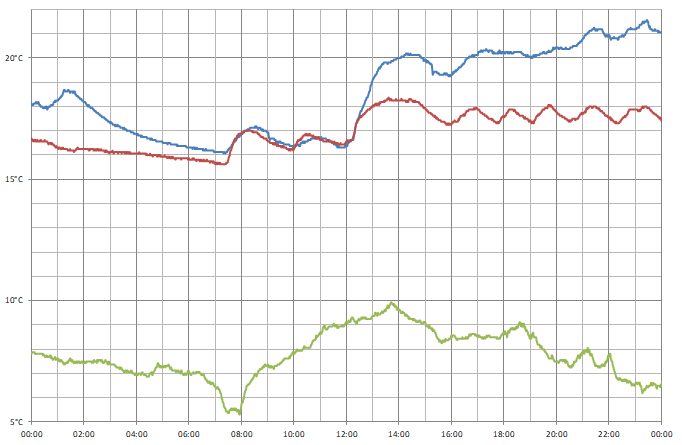
I captured data from three sensors over a 24 hour period; one outside (green line), one in my bedroom (red line) and one in my office (blue line). You can see how the central heating kicks in at 07:30, and I turned it up a little after 12:00. During the day the temperature in the bedroom moves up and down as the heating switches on and off, but the temperature in the office appears to be more consistent and a bit higher – the sensor is near where I am sitting and my desktop computer, which is likely contributing some heat.
Conclusion
What was originally intended to be a quick project to make use a couple of electronic components I had been sent in error soon turned into what I thought was an interesting demonstration of what can be done with the Cambridge Z88 using its stock software and some very basic additional hardware, further cementing my appreciation for the well-designed device.
The files accompanying this post can be downloaded below:
- ONEWIRE.BBC – 1-Wire demonstration program.
- TEMPLOG.BBC and TEMPLOG.CLI – Temperature logging program and CLI file to set up the alarm.
- templogs.zip and templogs.xlsx – Sample data captured by the temperature logging program.
SmartBox experimentation with DOS, RISC OS and C#/WinForms
Monday, 6th November 2023
My latest eBay purchase was influenced by a desire for some practical test/prototype equipment, a bit of nostalgia and a desire to learn something new.
A lot of my projects involve some sort of microcontroller running some software that will take inputs, perform decisions on them, and produce outputs. Getting to that stage tends to involve quite a lot of "boilerplate" hardware and software setup, and I'd quite like something that I can just plug in and get cracking with and write some quick test code instead of having to assemble a circuit on a breadboard or faff around with a clumsy IDE.
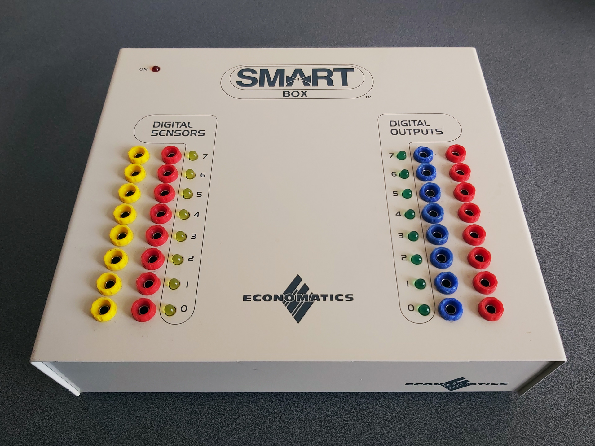
When I was at school in the 1990s one of the devices that got me into microcontrollers in the first place was a computer control system based around the Economatics SmartBox. This plugs into a computer via a serial connection, has eight simple digital inputs, eight simple digital outputs, four analogue inputs and four motor drivers. Programs could be written in a BASIC-like language or in flowchart form, and once you'd run and tested them on the SmartBox you could program them to a PIC microcontroller to run without the host computer.
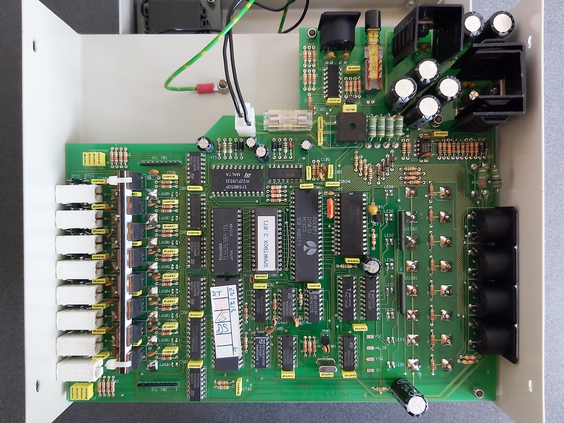
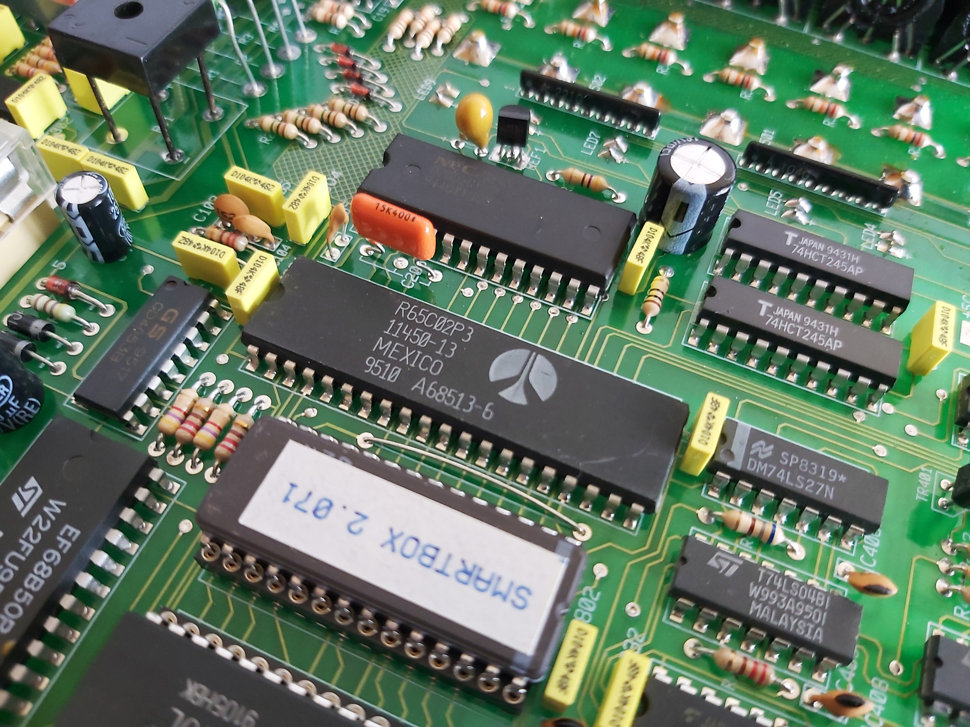
All along I'd assumed that the SmartBox was a simple interface box that relied on the host computer to do all of the processing, but doing some digging I found a thread on StarDot that delved into the heart of the machine and saw that there's a 65C02 CPU inside along with 32KB of RAM and the OS runs from a socketed 8KB ROM. As a long-term Z80 fan I thought it was time I should see how the other side lived – in spite of my fondness for the BBC Micro I don't own one and have not programmed any 6502 assembly, so a SmartBox seemed like it would also provide an affordable 6502 computer for experimentation.
Of course, one challenge was going to be finding the supporting software for the venerable SmartBox. Fortunately in the StarDot thread people had shared archives of the DOS, BBC Master and RISC OS software. One of the many handy features of DOSBox-X is its ability to connect an emulated serial port to a physical one in the host system, and so after building a serial cable for my SmartBox (using a pinout found, once again, via the StarDot thread) I was able to hook it up to my PC and get it working with SmartMove, the BASIC-like programming environment for the SmartBox.
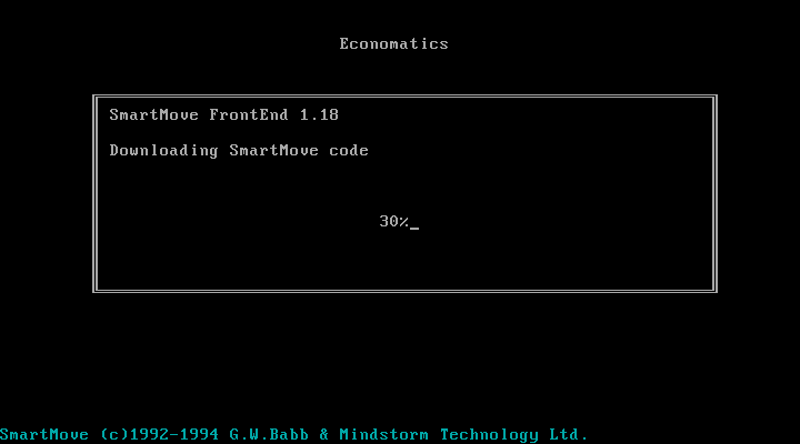
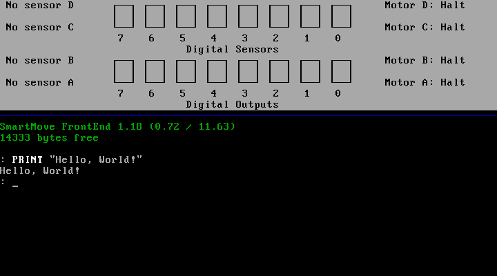
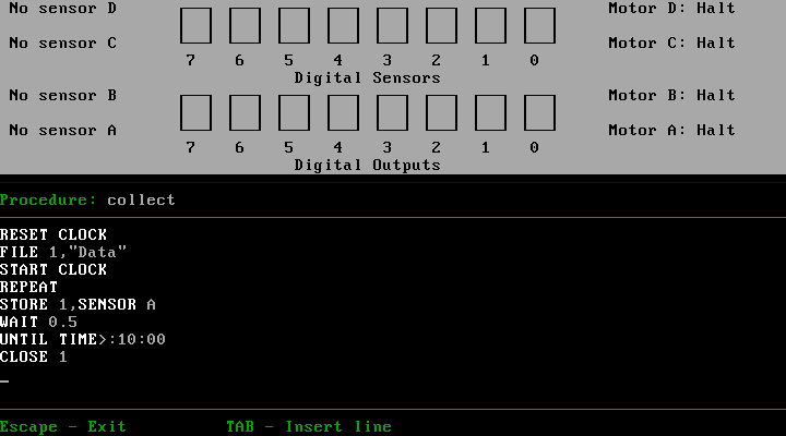
When the software is first run it needs to download SmartMove code into the SmartBox. This is because the programming environment and interpreter is actually running on the SmartBox itself, and the SmartMove software on the host PC is simply loading that interpreter onto the box (found in an accompanying file of 65C02 machine code named AL.COD) and then providing a user interface to that environment as a sort of terminal. This means you can close the SmartMove software (and unplug the serial cable) and your program will continue running on the SmartBox.
This ability to load and execute code directly on the SmartBox is one of the things that intrigued me as a way to get into 65C02 programming, but for the time being I was interested in digging deeper into the how the existing SmartMove software was interfacing with the box with the intention of writing a simple Z80 host interface that I could then adapt to the Cambridge Z88, my CP/M computer and maybe even the TI-83 Plus calculator series. Fortunately the documentation for the serial protocol used by SmartMove application has been documented so I was able to prototype a crude version of the software in C# using WinForms. It needs some serious tidying up before I can release it but as a basic test it does the job:
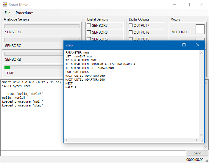
The ability to build new versions of the interface software for different platforms without needing to worry about porting over the BASIC interpreter seems sensible considering there were versions of SmartMove available for DOS, BBC Master, RISC OS and Apple Macintosh. All could use the same AL.COD but would just need to provide the relevant UI, input and output routines specific to their host platforms.
I had been using the DOS version of SmartMove as the initial inspiration of the user interface for my C#/WinForms implementation, however the screenshots of the RISC OS version in the user manual looked rather more visually appealing and an archived copy of this software was available. Unfortunately, I don't own an Acorn Archimedes, I was unable to get the software running properly on modern RISC OS on a Raspberry Pi (even with various compatibility shims in place) and I couldn't find an emulator that handled the serial port in a similar fashion to DOSBox-X. However, the excellent Arculator has source code available and armed with a copy of the 6651 UART datasheet I thought I'd have a go at hacking in the feature myself.
"Hack" is definitely the operative word and though my code is abominable it does work well enough to get the available RISC OS software working on my PC. It's downloadable from here and requires the addition of the host PC's serial port name to arc.cfg (e.g. serial_port = COM1).
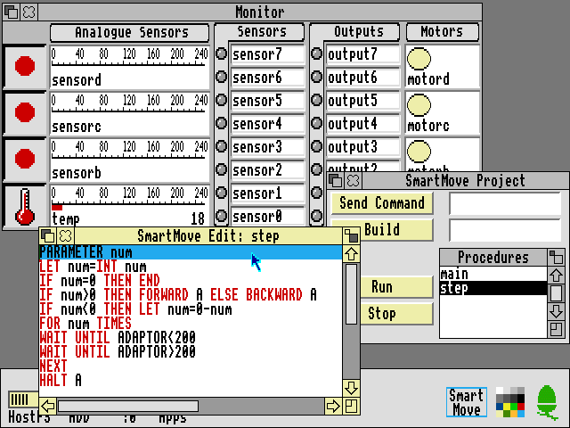
The above screenshot shows the RISC OS version of SmartMove which provided some additional inspiration for how a GUI version of the software should work. As I'd previously loaded some procedures onto the SmartBox via my C# version I could then bring the same procedures up for editing in the RISC OS version of the software. Handy!
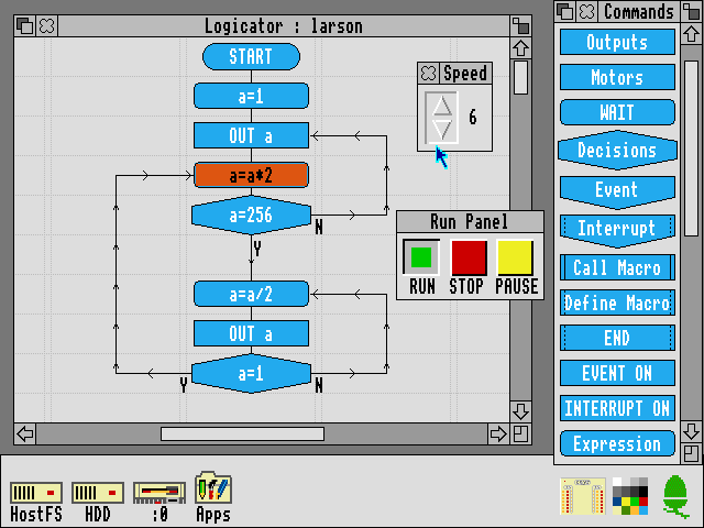
The Logicator software can be used to build programs using flowcharts instead of a BASIC-like programming language. As far as I'm aware Logicator directly accesses the inputs and outputs from a number of different host interface boxes and doesn't rely on 65C02 code loaded onto the box like SmartMove, but this does mean that when you close Logicator your program stops aas it's relying on the host PC to run the show. However, included with the archive of RISC OS software is an application called SmartFlow which first loads a flow chart "interpreter" into the SmartBox:
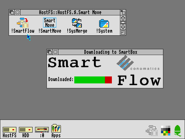
Once loaded you can then load a Logicator-format flowchart onto the SmartBox where it can be run without being connected to a host PC:
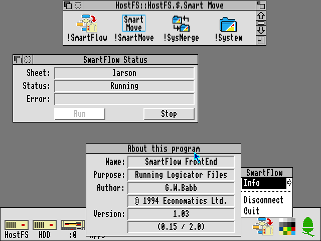
All in all it's been quite interesting to dig into the SmartBox and get a feel for how it works and what can be done with it. To this end I recorded a video demonstration of the SmartBox and its usage within RISC OS, though so far I feel I'm only really scratching the surface!
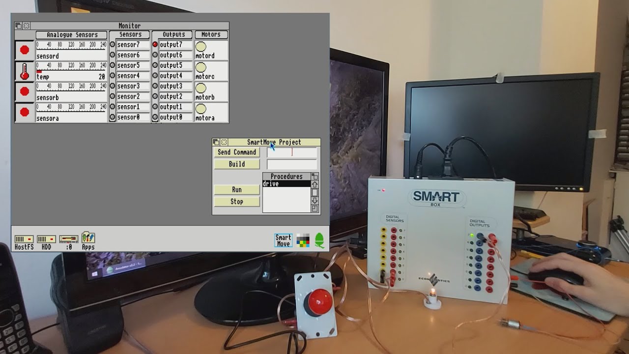
Adding 11KB of RAM to a CP/M 3 system with a single NAND gate chip
Wednesday, 30th August 2023
It's been quite a while since I posted about my Z80 Computer project. This is a home-made Z80 computer I built back in 2010 that features a 10MHz Z80 CPU with 64KB RAM that runs CP/M 3. It can drive an internal LCD, TV or VGA monitor at 320x240 (monochrome only) and unfortunately is a project I was never too happy with due to several compromises I had to make in its design – though at the time I was happy enough I got it to work at all! The video output was limited by both my choice to use an internal graphical LCD and the limitations of the dsPIC33F I chose to use to drive it and the software was all a bit half-baked. I could run the generic CP/M version of BBC BASIC on it, but this lacks graphics and sound support, for example.
More recently my work on adapting BBC BASIC to the Sega Master System had reignited my interest in 8-bit programming, though that too was imperfect due to the limitations of the Master System's VDP. I was further encouraged by coming third in the "Retro not Vintage" competition on /r/retrobattlestations, though I'm not sure I was quite worthy of a podium finish.
With this in mind I started work on improving the computer. I replaced the existing dsPIC33F VDP with a new one based around a dsPIC33E. This newer microcontroller has 32KB of RAM and can run at up to 70 MIPS, a big upgrade from the previous 16KB RAM and 40 MIPS. This provides me with enough video RAM to store the largest BBC Micro screen mode frame buffer (20KB) as well as the necessary CPU grunt to look up pixel data from colour palettes and output it to the screen. I've implemented all eight of the standard BBC Micro screen modes, from the high-res 640x256 (in two colours) MODE 0 to the low-res 160x256 (in sixteen colours) MODE 2 along with the Teletext-compatible MODE 7. This is all controlled via a BBC Micro-compatible VDU driver and the results all seem quite faithful with no real compromises.
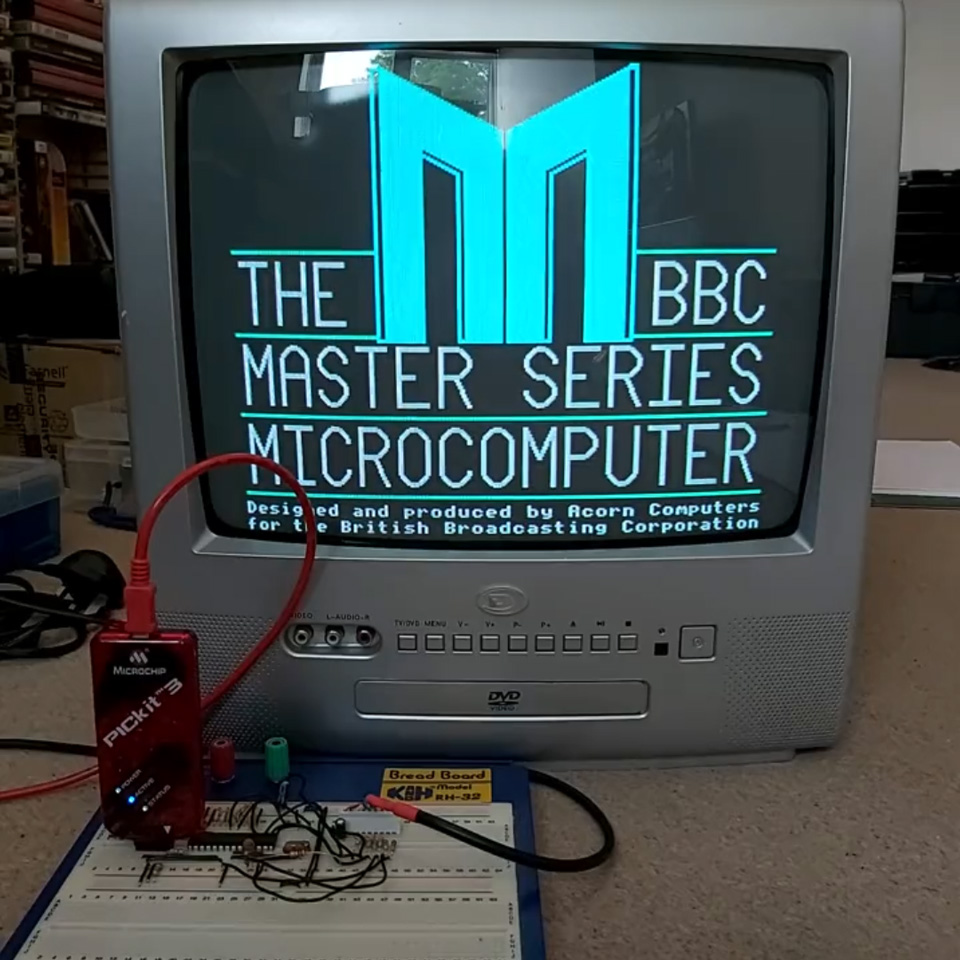
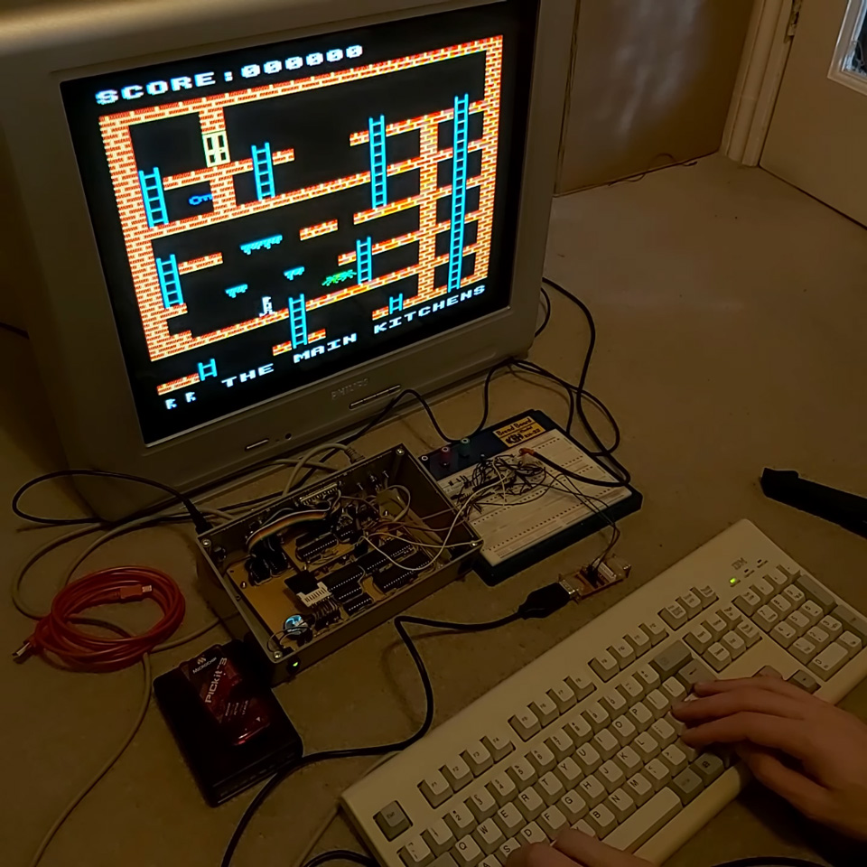
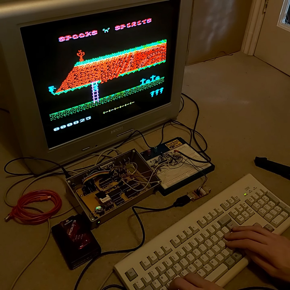
There was even enough CPU power left over on the microcontroller to implement BBC Micro-compatible SOUND and ENVELOPE, and with the source code for the CP/M version of BBC BASIC having been released since I last worked on the project it made it much easier to add all of the graphics and sound routines into the version of BBC BASIC specific to my computer.
To get an idea of what the computer is like to use, I recorded a little demo video here. However, this is not really what I wanted to write about in this post – I wanted to cover an easy way to free up some RAM by implementing banked CP/M 3.
Non-banked versus banked CP/M
I chose CP/M 3 as the OS for my computer instead of CP/M 2 as I'm using an SD card for storage and CP/M 3 has native support for disk sector sizes that do not directly match the file record size and it will handle the blocking/unblocking for you (CP/M's file records are 128 bytes long, SD card sectors are 512 bytes long). One other nice feature of CP/M 3 is the existence of a "banked" version which allows it to run on systems with more than 64KB of RAM. As far as user programs are concerned they still run in a flat 64KB memory space, however the OS can move certain parts of itself as well as disk and directory buffers into a separate memory bank where they are only accessed when needed, freeing up space in the "transient program area" (TPA). As well as more memory for user programs the banked version provides a much improved line editor when typing at the command-line, password protection of files and more descriptive error messages.
Naturally, when I read about this I thought it would be an obvious choice for my computer. As it is, I'm using a 128KB RAM chip but have tied A16 low as I didn't have any kind of MMU or bank-switching hardware setup (32KB and 128KB RAM chips are available in abundance, 64KB ones less so, and using a 128KB chip with the address line tied low involved a lot less soldering than two separate 32KB RAM chips). I did have an emulator where I could try to prototype the hardware changes to support a banked CP/M 3, however I was not able to get a banked version of the OS built and working so gave up – after all, I had a 49KB TPA, which seemed like it would be good enough.
With the other improvements to the computer recently I thought it worth reinvestigating. I did a bit of hunting to see if I could find any recommendations for a simple setup but most of what I could find ended up being a lot more complicated than what I was really looking for. After a bit more experimentation I was able to end up with a banked version of CP/M running on my computer and all I needed was a single NAND gate chip.
Memory requirements for banked CP/M
The memory layout of banked CP/M is actually quite a bit simpler than a lot of the threads I could find online seemed to make out. All you really need is a shared common area at the top of memory that will always be accessible regardless of the current state of the selected bank, and memory below that which can be switched between multiple banks. When booting the computer bank 0 will be selected, so both the common (resident) and banked parts can be copied to memory, and then bank 1 will be swapped in to provide the large TPA.
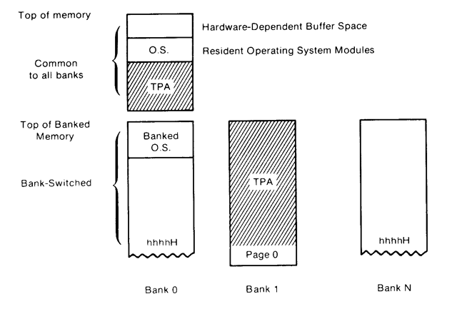
In my case, as I'm using a 128KB RAM chip, I will use A16 as the bank selection bit. When low this will provide access to the lower 64KB RAM on the chip, when high it will provide access to the upper 64KB RAM. To implement the common area at the top of memory, you then just need to check to see if the address is above the boundary between banked and common memory and if so to force A16 either high or low (it doesn't matter which, as long as it's consistent) so that when the address is in the common area the same bank will be accessed, regardless of the state of the bank selection bit.
Bank switching with simple logic
A simple way to implement a common area in upper memory is with AND (to detect the high address) and OR (to force the A16 high if it's a high address) logic, like this:
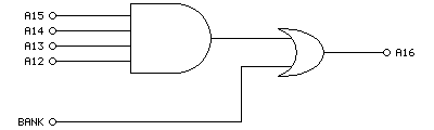
Here we use a 4-input AND gate to detect any memory address in the top 4KB of the chip (address lines A12 to A15 will go high at %1111000000000000 which gives a common region of $F000 to $FFFF). If that's the case, then the output of the 4-input AND gate will be high, which when ORed with the bank selection bit will force A16 high whenever we're in the common memory area. If we're below the common memory area then the value of the bank selection bit will pass through directly to A16, allowing us to bank switch the lower area of memory. Or, to summarise in a truth table:
| In | Out | ||||
|---|---|---|---|---|---|
| A12 | A13 | A14 | A15 | BANK | A16 |
| 1 | 1 | 1 | 1 | x | 1 |
| 0 | x | x | x | 0 | 0 |
| 0 | x | x | x | 1 | 1 |
| x | 0 | x | x | 0 | 0 |
| x | 0 | x | x | 1 | 1 |
| x | x | 0 | x | 0 | 0 |
| x | x | 0 | x | 1 | 1 |
| x | x | x | 0 | 0 | 0 |
| x | x | x | 0 | 1 | 1 |
However, it would be easier if we could implement this on a single chip. A 4x 2-input NAND gate chip (such as the SN74ALS00AN) should do the job when wired up as follows:
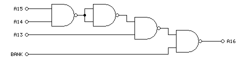
The truth table is a little different this time around:
| In | Out | |||
|---|---|---|---|---|
| A13 | A14 | A15 | BANK | A16 |
| 1 | 1 | 1 | x | 1 |
| 0 | x | x | 0 | 1 |
| 0 | x | x | 1 | 0 |
| x | 0 | x | 0 | 1 |
| x | 0 | x | 1 | 0 |
| x | x | 0 | 0 | 1 |
| x | x | 0 | 1 | 0 |
When accessing the banked region of memory A16 is the inverse of the bank selection bit. This doesn't matter, though, as long as there's a consistent mapping between logical addresses and the physical RAM addresses it will work even if it's "backwards". There's also one fewer address line, which means that the common area now runs from %1110000000000000 = $E000 to $FFFF, providing a common area of 8KB. In practice I didn't find this made a difference to the amount of memory available in the TPA; whether the common area was 4KB, 8KB or 16KB I was able to bring the TPA up to 60KB (from 49KB in the non-banked system), though it does eat into the amount of memory available on page 0 for disk and directory buffers. As I'm loading from an SD card (which is much faster than the floppy discs of yore) the reduced buffer space is less of a concern to me.
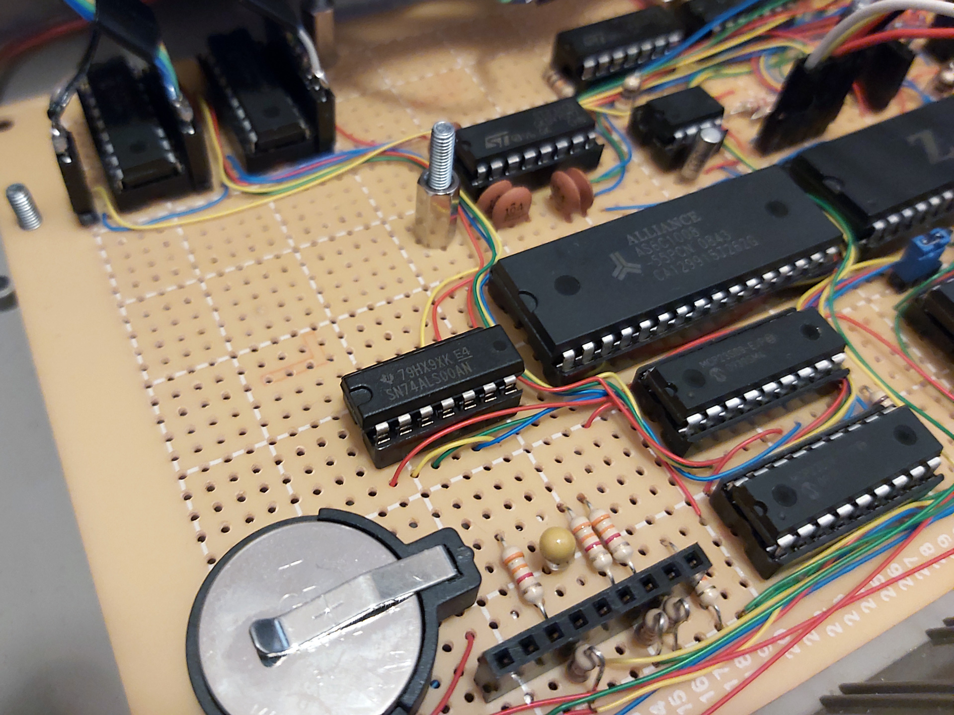
Fortunately there was enough space inside the computer (and a single remaining pin on the I/O controller to act thas bank selection bit) to add the NAND chip and drive A16. At last I have access to 120KB of my 128KB RAM chip... but what about the software?
Building a banked version of CP/M
I will start with the assumption that you have been able to build a non-banked version of CP/M 3 and got that running on your computer, as there is a lot less that can go wrong when doing so. Once you've got that working there's not too much to add to your BIOS to make it support banking, however I did run into a few issues with missing files and some misinterpretation of how things should work until I was able to get it working.
I used the "Developers Build Directory for CP/M 3" from The Unofficial CP/M Web site as my source for CP/M 3. This contains the GENCPM tool that will be used to generate the CPM3.SYS that will need to be loaded into memory by your boot loader. In my case I get my I/O controller to copy CP/M from the SD card into memory at boot – if you've already got the non-banked version of CP/M 3 booting then you'll be familiar with this, but do pay attention to table D-1 in the CP/M 3 system guide which points out the two parts of CP/M to load – the "resident" and "banked" portions. Both parts need to be loaded on a banked system, and both need to be loaded into page 0.
To get that far you will need to have relocatable copies of your banked BIOS (BNKBIOS3.SPR) and the BDOS (RESBDOS3.SPR and BNKBDOS3.SPR) ready to be used by GENCPM. I couldn't find a ready-made copy of these BDOS modules, but you can build them using RMAC and LINK as shown below:
RMAC RESBDOS
LINK RESBDOS3=RESBDOS[OS]
PIP BNKBDOS3.ASM=CPMBDOS2.ASM,CONBDOS.ASM,BDOS30.ASM
RMAC BNKBDOS3
LINK BNKBDOS3=BNKBDOS3[OS]
The banked BDOS source code is split between three different source files which need to be combined with PIP first, then can be built. For the sake of completeness, if you wanted to build the non-banked BDOS3.SPR you'd use a very similar set of commands, just with CPMBDOS1.ASM instead of CPMBDOS2.ASM:
PIP BDOS3.ASM=CPMBDOS1.ASM,CONBDOS.ASM,BDOS30.ASM
RMAC BDOS3
LINK BDOS3=BDOS3[OS]
The other important ingredient is your banked BIOS, BNKBIOS3.SPR. I don't get on with 8080 syntax so I assemble my BIOS3.MAC with Microsoft's M80 in Z80 mode (instead of RMAC).
RMAC SCB
RMAC BIOSKRNL
M80 =BIOS3
LINK BNKBIOS3[B]=BIOSKRNL,BIOS3,SCB
If you had previously edited BIOSKRNL.ASM to state banked equ false remember to change it to banked equ true as well!
The only additions you should need in your BIOS are implementations of ?xmove and ?bank. ?bank is an easy one, and just switches to the memory bank requested in the A register. In my case I handle that just by outputting A to the I/O port that handles bank switching:
; Select Memory Bank
; Entry Parameters: A=Memory Bank
; Returned Values:  None
; You must preserve or restore all registers other than the
; accumulator, A, upon exit.
?bank:
if banked
	out (bank$select),a ; change this for what your hardware requires
endif
	ret
(To retain compatibility with my old banked BIOS I wrap the changes in an if banked condition – banked equ true appears earlier in the file).
?xmove is a little more complicated – this states that the subsequent ?move operation (which copies BC bytes from DE to HL) should transfer data from one memory bank to another. Note that this only affects the next ?move operation; if ?move is called again afterwards without ?xmove then it should perform a copy within the same bank as before.
Fortunately the inter-bank copy is limited to 128 bytes so you can simply implement this by temporarily copying the data from one bank into a 128 byte buffer in common memory, then copying the data back to the destination bank. It's not exactly efficient, but it keeps the hardware simple.
; Memory-to-Memory Block Move
; Entry Parameters: HL=Destination address
;                   DE=Source address
;                   BC=Count
; Returned Values:  HL and DE must point to
;                   next bytes following move operation
?move:
	ex de,hl
	ldir
	ex de,hl
	ret

; Set Banks for Following MOVE
; Entry Parameters: B=destination bank
;                   C=source bank
; Returned Values:  None
?xmove:

if banked
	; Store the source/destination bank numbers
	ld (mov$src$b),bc
	; Make sure that the next call to move (via ?mov vector) uses the banked move routine.
	ld bc,banked$move
	ld (?mov+1),bc
	ret

banked$move:

	; Select source bank
	ld a,(mov$src$b)
	call ?bank

	; Swap registers from CP/M to Z80 conventions
	ex de,hl

	; Preserve destination and length
	push de
	push bc

	; Copy from source to buffer
	ld de,mov$buf
	ldir

	; Recover length and destination, preserve source
	pop bc
	pop de
	push hl

	; Select destination bank
	ld a,(mov$dst$b)
	call ?bank

	; Copy from buffer to destination
	ld hl,mov$buf
	ldir

	; Recover source
	pop hl

	; Swap registers from Z80 to CP/M conventions
	ex de,hl

	; Make sure that the next call to move (via ?mov vector) uses the regular move routine.
	ld bc,?move
	ld (?mov+1),bc
	ret

mov$src$b:
	db 0
mov$dst$b:
	db 0

mov$buf:
	ds 128
else
	; Unbanked
	ret
endif
This implementation works by changing the ?mov vector in the BIOSKRNL to point at our banked$move routine after a request to ?xmove. Once we've carried out the banked move, the original ?move routine is restored to the ?mov vector.
Once you have assembled and linked your BNKBIOS3.SPR, RESBDOS3.SPR and BNKBDOS3.SPR you can use GENCPM to create your new CPM3.SYS. You'll need to answer some questions differently to support the banked system:
- Bank switched memory? Y.
- Common memory base page? E0 (if using the NAND gate circuit above – our common area starts at $E000).
- Number of memory segments? 1 – we have three in total (bank 0, bank 1 and common) however bank 1 and common are not included in the segment table so should be ignored here.
- Memory segment table base, size, bank: 01, 90, 00 (we want to keep CP/M out of the "zero page" so start the segment from $0100, CP/M 3 starts at $9100 so we have $9100-$0100=$9000 as our size, the bank number is 0).
Before being prompted for the memory segment table GENCPM will display where CP/M 3 itself is using memory so you can use that to figure out how much free space you have on your bank zero for your segment definition. However, if you enter a value that is too large GENCPM will automatically reduce the size for you.
After this you will be prompted to create disk and directory buffers for each of your disk definitions – pay attention to available space to get an idea of how many buffers you can create, but if in doubt just allocate a single buffer for each disk/directory as prompted as that will at least get you booted, then you can experiment with larger buffers later.
I did intentionally start my segment from $0100 instead of $0000 and this is to avoid problems with interrupts and to keep the zero page free. My computer design uses interrupts to signal to the Z80 that keys are available (for example) instead of requiring it to constantly poll the I/O controller. However, I did find that if I interrupted the CPU (e.g. by pressing a key) when it had switched over to page 0 it would hang the computer as the ISR vector had been switched out from underneath it. My ISR is in common memory and I just make sure that when the computer boots it installs its interrupt vectors in every memory bank so that it doesn't matter which is currently swapped in, it'll always find its way to the common ISR.
After making these changes I was greeted with a 60KB TPA instead of the previous 49KB TPA – 11KB of extra memory is well worth it, and the improved line editor in CP/M 3 is another nice bonus. I did think that implementing this was going to be a nightmare, but in the end I only needed one extra NAND gate and a few easy changes to the software.
Addendum (31st August 2023): One other change you will need to implement is to support disk operations reading from or writing to specific memory banks. I forgot to mention this earlier as it's handled by the setbnk routine inside BIOSKRNL, and that routine stores the selected DMA bank number in the @dbnk variable. When your BIOS performs a disk read or write operation it will need to preserve the current bank number, switch to the bank number in @dbnk, carry out the read or write operation, then restore the previous bank number.
In my case, disk I/O is handled by the AVR I/O controller where operations are set up by sending over the DMA address, sector and track numbers, drive index and then performing a read from either the "read" or "write" ports to initiate the I/O operation and retrieve the status. The only change required was to make sure that the bank number is also sent over before initiating the I/O request so the AVR knows which bank it should be accessing:
fd$copy$ptrs:

	ld hl,(@dma)
	ld a,l
	out (disk$dma$l),a
	ld a,h
	out (disk$dma$h),a

	ld hl,(@sect)
	ld a,l
	out (disk$sector$l),a
	ld a,h
	out (disk$sector$h),a

	ld hl,(@trk)
	ld a,l
	out (disk$track$l),a
	ld a,h
	out (disk$track$h),a

	ld a,(@adrv)
	out (disk$drive),a

	if banked
		ld a,(@dbnk)
		out (disk$dma$bank),a
	endif

	ret

fd$write:
	call fd$copy$ptrs
	in a,(disk$write)
	ret

fd$read:
	call fd$copy$ptrs
	in a,(disk$read)
	ret
I'm pretty sure I didn't forget anything else!
Reverse engineering Z-Tape for the Cambridge Z88
Saturday, 10th June 2023
When reading about the Cambridge Z88 computer and its available software I bumped into the occasional mention of Z-Tape by Wordmongers, a system that allowed you to back up files from your Z88 to a cassette recorder. I had wondered how this worked, assuming there some sort of external hardware to connect the cassette recorder to the Z88 (likely via its serial port). I'd done some work on tape loading and saving myself for the Sega Master System and had come up with a somewhat hacky but minimal solution that relies on abuse of a hex inverter. Surely a commercially-released product would have a better way of doing things, or at least so I thought!
More recently I noticed someone had uploaded a copy of the application and some accompanying documentation to the Cambridge Z88 page on SourceForge, so I downloaded it to take a look and was very surprised at what I found:
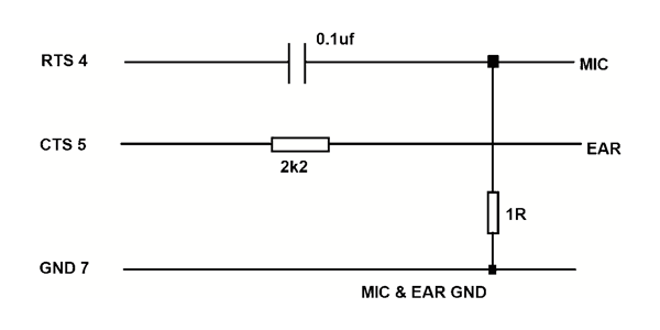
That can't work, surely? The output for recording seems sensible enough, using the 1Ω resistor to ground on the output to reduce the level down to something that could be fed into a sensitive microphone input, but just running the earphone output directly into the RS-232 port's CTS line doesn't seem like it would do the job. There's only one way to find out, though, and that's to build a cable and try it out and to my surprise it does indeed work!
I have had a few issues with this, however. The program appears to require that the phase of the data played back into the Z88 matches the phase that it was recorded. Both of my cassette recorders reverse the phase when playing back the recordings. Fortunately one of them does have a phase reversal switch, and two wrongs in this case does make a right and by setting the phase switch to "reverse" it allows Z-Tape to load back the recorded data.
The overall loader is not particularly reliable, though. It relies on a very strong output from the cassette recorder to successfully register a signal on the Z88's serial port, and I find I have to rewind to try again quite often. That it works at all with such a simple cable is certainly impressive, though.
In my testing I wrote a little BASIC program that crudely checks the signal level on the RS-232 input. You can use this to test the strength of your cassette recorder's output: it will display a rolling progress bar with the approximate signal strength. With my cassette recorder I can get over 80% when playing back a block, but I can't register anywhere near that when connecting the Z88 to my PC's audio output or my phone's headphone socket and consequently can't load back recordings from those devices.
10 *NAME Tape Level Test
20 REPEAT
30   S%=0
40   FORI%=0TO99:S%=S%+(GET(&E5)AND1):NEXT
50   S%=50-ABS(50-S%)
60   PRINT'S%*2;"% ";CHR$1;"R";CHR$1;"3N";CHR$(32+S%);" ";CHR$1;"G";CHR$1;"3N";CHR$(32+(50-S%));" ";CHR$1;"3-RG ";
70 UNTIL INKEY(0)<>-1
80 PRINT
Once I'd experimented with Z-Tape and a cassette recorder I thought it would be interesting to see how it worked and whether I could reverse-engineer the format used. I connected the Z88 to my PC, made some recordings, and then set to work.
Bit-level format
The first thing to do is to establish the base frequency. After taking a recording from the Z88, I checked it in Audacity's frequency analyser and found a strong peak at 1590Hz:
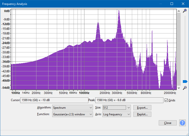
There is also a strong peak at 3195Hz, which is very close to twice the other peak's frequency (halving it gives us 1597.5Hz, close to 1590Hz). Based on these measurements it would seem that the base frequency is around 1600Hz, and likely that the tape format is a combination of 1600Hz and 3200Hz tones. Zooming into the recorded waveform shows the two different tones:
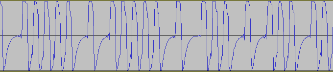
A common way to record data on tape is to use one full cycle of the base frequency to represent a "0" bit and two full cycles of twice the base frequency to represent a "1" bit. This means that the data is the same length regardless of how many "0"s or "1"s appear in the data, and looking at the length of data blocks in the recording they were all the same length, so it seems this is a possible candidate.
The phase of the signal is also important. If we represent the signal as a sine wave, a phase of 0° would start at zero, increase in the positive direction for the first quarter of the wave, head down in the negative direction for the next half of the wave, before returning to zero in a positive direction in the last quarter of the wave. Conversely a phase of 180° would start from zero but go negative in the first half of the wave before going positive in the second half of the wave. The phase can be determined by looking at the start of the signal after a period of silence:
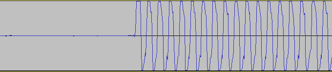
As the signal goes positive first after a period of silence we can confirm the signal has a phase of 0°. In summary, the bit-level format required by Z-Tape is as follows:
- Base frequency of 1600Hz.
- Phase of 0°.
- "0" bits encoded as one full cycle at base frequency (1600Hz).
- "1" bits encoded as two full cycles at twice the base frequency (3200Hz).
Block-level format
Now that we have a stream of bits, we can group them into blocks of data on the tape. Each block starts with a leader or pilot tone, which is effectively a long stream of "1" bits (3200Hz). This lasts 1.25 seconds, after which there is a very brief silence (around two full waves in length) followed by the stream of bits that make up the actual block data.
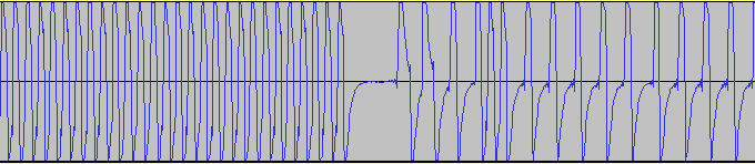
I created some files on the Z88 that followed certain obvious patterns, for example a file that alternated $00 bytes and $FF bytes so you'd expect to see eight consecutive "0" bits in the recording followed by eight consecutive "1" bits. This would help check to see if there were any start, stop or parity bits in the data (or if it was just eight plain bits of data). I also had a file that contained all of the numbers from $00 to $FF consecutively, so you'd be able to see a clear pattern of byte values counting up and use this to check whether the data was sent least-significant or most-significant bit first.
Using these files I quickly found that the data in each block always starts with two zero bits (immediately after the leader or pilot tone) and is then sent in plain 8-bit bytes (no start, stop or parity bits) with the least significant bit sent first. Each block always contains 1031 bytes of raw data, no matter the size of the file being transmitted. I knew that there was a checksum as Z-Tape would occasionally grumble when loading about a checksum error and I could see that after transferring small files there'd be data at the start of the block, a gap filled with zeroes, followed by a final non-zero data byte. I assumed this was the checksum, and found that by adding up all 1031 bytes in the block the result always came to zero. The checksum can therefore be calculated by setting a counter to zero, subtracting the value of every byte in the 1030 data bytes of the block, and then appending the counter value to as the 1031st byte of the block.
In summary, the block-level format is as follows:
- 1.25 seconds of 3200Hz leader or pilot tone (stream of "1" bits).
- Silence for the duration of two full cycles.
- Two "0" bits, sent as two full cycles of the 1600Hz tone.
- 1030 data bytes, each sent as eight plain bits, least significant bit first.
- "0" bits sent as one full cycle of 1600Hz tone.
- "1" bits sent as two full cycles of 3200Hz tone
- Checksum data byte, sent in same manner as other data bytes, but calculated such that adding up all 1031 data bytes in the block results in 0.
There is approximately half a second of silence between data blocks, though the actual amount of time depends on how much work the Z-Tape application has to do to prepare each block. When building the catalogue before sending a large number of files I've seen gaps over 24 seconds long!
Block contents
Each block always contains 1030 bytes of data plus a checksum byte, and for the sake of simplicity I'll ignore the checksum in the discussion below.
The first byte of each block's data determines what sort of block it is. I've identified six different block types.
The next two bytes are the size of the data included in the block, least significant byte first, though sometimes this value is incorrect or missing depending on the particular type of block.
After that are two bytes that record the block number, least significant byte first. The first block has a block number of 0 and this counts up one for every block on the tape.
After this you'll find the actual data associated with the block, normally up to 1024 bytes, with the rest of the block padded with zeroes.
Blocks $04 and $05: Catalogue blocks
When storing a selection of files on tape Z-Tape writes a catalogue file first containing a list of files. The final block in the catalogue is sent with a block type of $05, if more than one block is required to represent the catalogue then preceding partial catalogue blocks use a type of $04.
Catalogue blocks always have a reported size field of zero.
Each file entry is stored in a record 28 bytes long. As each block can store up to 1025 bytes of user data this allows for up to 36 files to be described in each catalogue block.
The records always start from offset 5 into the block (one byte block ID, two byte size = 0, two byte block number) and each takes the following format:
- Bytes 0~15: Filename.
- Byte 16: 0 (NUL terminator for filename).
- Bytes 17~21: File size as floating-point number (four byte mantissa, MSB first, followed by exponent).
- Bytes 22~24: Three byte time (centiseconds since start of day, LSB first).
- Bytes 25~27: Three byte Julian date (number of days since Monday 23rd November 4713 BC, LSB first).
Filenames can be up to sixteen characters long (12 filename characters, a dot, three extension characters). They can be mixed case.
The file size being a floating-point number took me a while to figure out! This is the numeric format used by BBC BASIC (Z80) and is also internally used by the Z88 OS for its FPP routines. The format for this number can be found in the BBC BASIC documentation, though for the sake of simplicity if you're creating your own catalogue in Z-Tape format note that it does accept the "special case" real number where the exponent is set to 0 and the mantissa is a regular integer. If you're decoding tapes created by Z-Tape you'll need to decode the floating-point number yourself, though.
The date and time are in the format used internally by the Z88 OS. The only challenge here is the Julian day is outside the range that can be represented by some programming language date and time functions which can complicate matters. Here's a snippet of C# that works if you're trying to convert a catalogue date and catalogue time to a .NET DateTime object:
var catalogueDate = DateTime.FromOADate(catalogueDateNum - 2415019);
catalogueDate = catalogueDate.AddMilliseconds(catalogueTimeNum * 10);
Blocks $01 and $06: File start blocks
These blocks appear at the start of a file. Block type $06 is used if the whole file data can fit in a single block, $01 if additional blocks containing the rest of the file will follow.
The block size is used here to determine how many bytes of data are present. This will be the size of the whole file if the block type is $06, $03E0 (992 bytes) if the block type is $01.
Block bytes from 5 to 31 contain a copy of the filename, padded with zeroes. This must be in UPPERCASE, regardless of how the file was listed in the catalogue, otherwise the Z-Tape loader will be unable to recognise the file by name (this one took a while to puzzle out!)
After this comes the file data. If this is a block type $06 that's the end of it, but if it's block $01 more file data will follow...
Block $02 and $03: File data blocks
These blocks contain raw file data from offset 5 (there is no filename field, as with blocks $01 and $06) and appear in the middle or end of files. If the block type is $02 then this block appears in the middle of the file and it always contains 1024 bytes of data, though the header will report it contains $03E0 (992 bytes) and should be ignored. If it's block type $03 then that corresponds to the end of the file, and the data length should be taken into consideration.
Block types summary
The following table documents the block types. All multi-byte numeric values are transmitted least significant byte first with the exception of the floating-point numbers representing the file sizes in the catalogue described earlier.
| Offset | Catalogue | File | ||||
|---|---|---|---|---|---|---|
| Partial catalogue block | Final catalogue block | File fits in single block | First file block | Middle file block | Last file block | |
| 0 | $04 | $05 | $06 | $01 | $02 | $03 |
| 1~2 | $0000 | Data length | $03E0 | Data length | ||
| 3~4 | Block number (starting from 0 for the first block) | |||||
| 5 | Up to 36 28-byte records listing the files about to follow. | The UPPERCASE name of the file, zero-padded to 27 bytes in length. | 1024 bytes of file data. | Data length bytes of file data. | ||
| 32 | Data length bytes of file data. | |||||
| 1030 | Checksum calculated so that adding up all 1031 bytes results in 0. | |||||
Creating Z-Tape audio on a PC
This is all well and good, but what's the point of it? The information above may be useful if someone has an old tape that they needed to recover data from but no longer had a Z88, though that seems like a fairly remote possibility. Another possibility could be to create Z-Tape data from files on PC and then play it back to transfer data from the PC to the Z88. Alternatively, a selection of programs could be stored on a CD and loaded onto the Z88 from a portable CD player when out and about.
Maybe not the most useful ideas, but here's a C# function that will take an array of filenames and generate a series of data blocks in the Z-Tape format, including a catalogue:
static byte[][] CreateBlocksFromFiles(string[] files) {

    List<byte[]> blocks = new List<byte[]>();

    // generate the catalogue
    for (int firstFileInBlock = 0; firstFileInBlock < files.Length; firstFileInBlock += 36) {

        // which is the last file in the block (+1) that we will write to the file?
        var lastFileInBlock = Math.Min(files.Length, firstFileInBlock + 36);

        // catalogue block data is 1030 bytes, same as all other blocks
        var catalogue = new byte[1030];

        // if the is the last block in the catalogue, block type is 0x05, otherwise it's 0x04
        catalogue[0] = (byte)((lastFileInBlock == files.Length) ? 0x05 : 0x04);

        // current block number
        catalogue[3] = (byte)(blocks.Count >> 0);
        catalogue[4] = (byte)(blocks.Count >> 8);

        // write each file for this block to the catalogue
        var catalogueOffset = 5;
        for (int fileInBlock = firstFileInBlock; fileInBlock < lastFileInBlock; ++fileInBlock) {

            var file = new FileInfo(files[fileInBlock]);

            // file name (can be mixed case)
            Array.Copy(Encoding.ASCII.GetBytes(file.Name.PadRight(16, '\0')[..16]), 0, catalogue, catalogueOffset, 16);

            // file size (Z-Tape normally uses floating-point values)
            catalogue[catalogueOffset + 17] = (byte)(file.Length >> 24);
            catalogue[catalogueOffset + 18] = (byte)(file.Length >> 16);
            catalogue[catalogueOffset + 19] = (byte)(file.Length >> 8);
            catalogue[catalogueOffset + 20] = (byte)(file.Length >> 0);

            // file date/time
            var writeTime = file.LastWriteTime;

            // time is centiseconds since midnight
            var fileTime = (int)(writeTime.TimeOfDay.TotalMilliseconds / 10);
            catalogue[catalogueOffset + 22] = (byte)(fileTime >> 0);
            catalogue[catalogueOffset + 23] = (byte)(fileTime >> 8);
            catalogue[catalogueOffset + 24] = (byte)(fileTime >> 16);

            // date is Julian day number
            var fileDate = (int)(writeTime.ToOADate() + 2415019);
            catalogue[catalogueOffset + 25] = (byte)(fileDate >> 0);
            catalogue[catalogueOffset + 26] = (byte)(fileDate >> 8);
            catalogue[catalogueOffset + 27] = (byte)(fileDate >> 16);

            catalogueOffset += 28;
        }

        blocks.Add(catalogue);

    }

    // write each file to the tape
    foreach (var filePath in files) {

        var file = new FileInfo(filePath);

        using (var fileData = file.OpenRead()) {
            do {

                var fileBlock = new byte[1030];

                // current block number
                fileBlock[3] = (byte)(blocks.Count >> 0);
                fileBlock[4] = (byte)(blocks.Count >> 8);

                // how much data can we store in the block?
                var maxBlockData = 1024;
                var blockDataOffset = 5;

                if (fileData.Position == 0) {

                    // if it's the first block for the file, store the filename (must be UPPERCASE)
                    Array.Copy(Encoding.ASCII.GetBytes(file.Name.ToUpperInvariant().PadRight(16, '\0')[..16]), 0, fileBlock, blockDataOffset, 16);
                    blockDataOffset = 0x20;

                    // can't store as much in the first block due to all the header info we just wrote
                    maxBlockData = 992;

                    // what sort of block is it?
                    if (file.Length > maxBlockData) {
                        fileBlock[0] = 0x01; // first block in a multi-block file
                    } else {
                        fileBlock[0] = 0x06; // single block for the whole file
                    }

                } else {

                    // what sort of block is it?
                    if (file.Length > fileData.Position + maxBlockData) {
                        fileBlock[0] = 0x02; // continued data block in a multi-block file
                    } else {
                        fileBlock[0] = 0x03; // last data block in a multi-block file
                    }

                }

                // how much data can we actually copy?
                var actualBlockData = Math.Min(maxBlockData, (int)(file.Length - fileData.Position));

                // read the data
                if (fileData.Read(fileBlock, blockDataOffset, actualBlockData) != actualBlockData) {
                    throw new InvalidDataException();
                }

                // store the data size
                fileBlock[1] = (byte)(actualBlockData >> 0);
                fileBlock[2] = (byte)(actualBlockData >> 8);

                blocks.Add(fileBlock);

            } while (fileData.Position < fileData.Length);
        }

    }

    return blocks.ToArray();
}
Once the blocks have been generated, we can convert them to a tape format like UEF:
static void WriteUef(string filename, IEnumerable<byte[]> blocks, ushort baudRate = 1600, bool reversePhase = false) {

    using (var uefFile = File.Create(filename))
    using (var uefWriter = new BinaryWriter(uefFile)) {

        // Header
        uefWriter.Write(Encoding.ASCII.GetBytes("UEF File!\0"));
        uefWriter.Write((byte)0x0A); // minor version
        uefWriter.Write((byte)0x00); // major version

        // Chunk &0113 - change of base frequency
        uefWriter.Write((ushort)0x0113);
        uefWriter.Write((uint)4);
        uefWriter.Write((float)baudRate);

        // Chunk &0115 - change of phase
        uefWriter.Write((ushort)0x0115);
        uefWriter.Write((uint)2);
        uefWriter.Write((ushort)(reversePhase ? 180 : 0));

        // Write each block to the UEF
        foreach (var block in blocks) {

            // Calculate the checksum
            byte checksum = 0;
            foreach (var b in block) {
                checksum -= b;
            }

            // Chunk &0110 - carrier tone
            uefWriter.Write((ushort)0x0110);
            uefWriter.Write((uint)2);
            uefWriter.Write((ushort)(baudRate * 5 / 4));

            // Chunk &0112 - integer gap
            uefWriter.Write((ushort)0x0112);
            uefWriter.Write((uint)2);
            uefWriter.Write((ushort)2);

            // Chunk &0102 - explicit tape data block
            uefWriter.Write((ushort)0x0102);
            uefWriter.Write((uint)2);
            uefWriter.Write((byte)14); // bit count = (chunk length * 8) - 14 = 2 bits
            uefWriter.Write((byte)0); // 2 zero bits

            // Chunk &0102 - explicit tape data block
            uefWriter.Write((ushort)0x0102);
            uefWriter.Write((uint)(2 + block.Length));
            uefWriter.Write((byte)8); // bit count = (chunk length) * 8 - 8
            uefWriter.Write(block);
            uefWriter.Write(checksum);

            // Chunk &0112 - integer gap
            uefWriter.Write((ushort)0x0112);
            uefWriter.Write((uint)2);
            uefWriter.Write((ushort)(baudRate / 2));
        }
    }

}
A .wav file is probably an easier format to work with, however!
static void WriteWav(string filename, IEnumerable<byte[]> blocks, int baudRate = 1600, bool reversePhase = false, uint sampleRate = 48000, uint channelCount = 1, ushort bitsPerSample = 16) {

    // generate cycles
    var cycleSampleCount = sampleRate / baudRate;

    var bits = new byte[3][]; // good old ternary logic - true, false, and file_not_found.

    for (int b = 0; b < 3; ++b) {
        bits[b] = new byte[cycleSampleCount * bitsPerSample / 8 * channelCount];
    }

    for (int c = 0; c < cycleSampleCount * channelCount; ++c) {
        double a = ((c / channelCount) * Math.PI * 2.0d) / cycleSampleCount;

        for (int b = 0; b < 3; ++b) {

            double v = b == 2 ? 0 : Math.Sin(a * (1.0d + b));

            if (reversePhase) v = -v;

            switch (bitsPerSample) {
                case 8:
                    bits[b][c] = (byte)Math.Round(Math.Max(byte.MinValue, Math.Min(byte.MaxValue, 127.5d + 127.5d * v)));
                    break;
                case 16:
                    short vs = (short)Math.Round(Math.Max(short.MinValue, Math.Min(short.MaxValue, (short.MaxValue + 0.5d) * v)));
                    bits[b][c * 2 + 0] = (byte)(vs >> 0); bits[b][c * 2 + 1] = (byte)(vs >> 8);
                    break;
            }
        }
    }


    using (var wavFile = File.Create(filename))
    using (var wavWriter = new BinaryWriter(wavFile)) {

        // RIFF header
        wavWriter.Write(Encoding.ASCII.GetBytes("RIFF")); // chunk ID

        var riffDataSizePtr = wavFile.Position;
        wavWriter.Write((uint)0); // file size (we'll write this later)

        wavWriter.Write(Encoding.ASCII.GetBytes("WAVE")); // RIFF type ID

        // chunk 1 (format)
        wavWriter.Write(Encoding.ASCII.GetBytes("fmt ")); // chunk ID
        wavWriter.Write((uint)16); // chunk 1 size
        wavWriter.Write((ushort)1); // format tag
        wavWriter.Write((ushort)channelCount); // channel count
        wavWriter.Write((uint)sampleRate); // sample rate
        wavWriter.Write((uint)(sampleRate * channelCount * bitsPerSample / 8)); // byte rate
        wavWriter.Write((ushort)(channelCount * bitsPerSample / 8)); // block align
        wavWriter.Write((ushort)bitsPerSample); // bits per sample

        // chunk 2 (data)
        wavWriter.Write(Encoding.ASCII.GetBytes("data")); // chunk ID
        var waveDataSizePtr = wavFile.Position;
        wavWriter.Write((uint)0); // wave size (we'll write this later)

        var waveDataStartPtr = wavFile.Position;

        // write half a second of silence
        for (int i = 0; i < baudRate / 2; ++i) {
            wavWriter.Write(bits[2]);
        }

        // Write each block to the WAV
        foreach (var block in blocks) {

            // write 1.25 seconds of carrier tone
            for (int i = 0; i < baudRate * 5 / 4; ++i) {
                wavWriter.Write(bits[1]);
            }

            // write gap
            wavWriter.Write(bits[2]);
            wavWriter.Write(bits[2]);

            // write two 0 bits
            wavWriter.Write(bits[0]);
            wavWriter.Write(bits[0]);

            // calculate the checksum as we go
            byte checksum = 0;

            // write all of the bytes in the block
            for (var i = 0; i < block.Length + 1; ++i) {

                // fetch the byte to write
                byte b;

                if (i < block.Length) {
                    // use data from the block and update the checksum
                    b = block[i];
                    checksum -= b;
                } else {
                    // write the checksum
                    b = checksum;
                }

                // write each bit, LSB first
                for (int bit = 0; bit < 8; ++bit) {
                    wavWriter.Write(bits[b & 1]);
                    b >>= 1;
                }
            }

            // write half a second of silence
            for (int i = 0; i < baudRate / 2; ++i) {
                wavWriter.Write(bits[2]);
            }
        }

        // update wave size
        var waveDataEndPtr = wavFile.Position;

        wavFile.Seek(waveDataSizePtr, SeekOrigin.Begin);
        wavWriter.Write((uint)(waveDataEndPtr - waveDataStartPtr));

        // update RIFF size
        wavFile.Seek(riffDataSizePtr, SeekOrigin.Begin);
        wavWriter.Write((uint)(waveDataEndPtr - 8));

    }

}
But, I hear you say, didn't you earlier mention how a PC's audio output was now powerful enough to drive the Z88's serial port? I did indeed, and that's why I've also put together this little circuit:
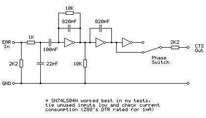
This is based on the tape interface circuit I devised for the Sega Master System and uses an SN74LS04N hex inverter chip as an amplifier to drive the Z88's CTS line. It's designed to be powered from the Z88's serial port which provides 5V at 1mA on the DTR pin. This current limit does seem awfully low and I have seen it reported as 10mA in some places but I'm not sure if that's a typo or not — the user manual states 1mA. In my testing this circuit consumes between 2mA-3mA which is much more than 1mA but it does still work, however I would strongly recommend doing your own testing before hooking anything up to your Z88's serial port. The other hex inverter chips I tried all consumed over 20mA in this use which is far too much for the Z88! There was a noticeable difference in current consumption depending on whether unused inputs were tied high or tied low, so please do your own testing.
The presence of a phase switch does allow this circuit to be used with recorders that reverse the phase when recording but don't provide a phase reversal switch of their own to fix this on playback.
All in all I'm very impressed that the Z-Tape software works as well as it does considering the simplicity of the hardware, and it's been a lot of fun digging into how it works.
Using a VDrive to access USB flash drives from a Cambridge Z88
Saturday, 13th May 2023
The VDrive is a handy module for electronic projects that need to access files on a USB flash drive. It's based around a USB host microcontroller and comes preinstalled with some firmware that provides control over the drive with simple commands sent via a serial connection (UART or SPI).
A few years ago I started putting together some code to connect the module to my Cambridge Z88 computer. All I needed was a way to power the drive and a MAX232 chip to translate the computer's RS-232 interface to the VDrive's logic levels, and after around 150 lines of BBC BASIC I had a program that could show directory listings, let me browse folders, and fetch files from the USB drive to the Z88's file system.
This worked well enough but was a bit clumsy. For example, to maintain good performance rather than alternate between reading a single byte from the drive and writing it to the local file system it's better to read and write larger chunks at a time. BBC BASIC doesn't provide a built-in way to do that, though you can read or write CR-terminated strings. When you read each part of the file this way you therefore need to decide whether the string you've just read is a certain length because you've reached a CR terminator (which isn't included in the read string), whether you've reached the end of the file, or whether the string buffer is full, and from that piece the file back together. I got this working quite well but it's still fundamentally an inelegant hack. Doing it properly would require some assembly code, and that would also be required for some other operations (such as properly transferring date and time modification information) that are otherwise not possible from pure BASIC.
Fortunately, BBC BASIC has a built-in assembler and that makes integration of assembly code in BASIC programs quite a bit easier than it would otherwise be. However, as I considered the amount of assembly code required would be quite high, I thought it might be more sensible to just rewrite the program as a native Z88 popdown application.

Status dialog shown when fetching a file from the drive
This is what I ended up doing, and it can be downloaded from its product page. It was quite a lot of fun to learn my way around the Z88's OS – not just for things like file handling, date and time manipulation, and integration with menu and help system but for some of the challenges involved in writing Z80 code for a system that shares memory between multiple running applications (and the file system) rather than my usual environment of having a big block of contiguous RAM to do whatever I fancied in.
The directory listing is the most obvious place where I had to rely on dynamic memory allocation. Each file or folder name being sent in a directory listing by the VDrive is allocated its own memory and I arranged the names together in a linked list that is sorted with an insertion sort.
Being my first Z88 application it's not especially well written but I've been using it for a while now and it seems to work well enough so I've released it, both on this very website and on GitHub.
Take your TI-83 Plus online with a TIWiFiModem
Monday, 27th March 2023
One of the issues holding me back with my development of the Light Gun Commando project (aside from a lack of free time due to the day job) was running out of prototyping breadboards and the difficulty of swapping between different console adaptor boards for testing.
Normally by this point I'd have started soldering together more permanent prototypes on little circuit boards, but I've been having a difficult time with the boards I've got in stock apparently being made of a metal that's impossible to solder to. They were very cheap, but for some reason the solder joints would end up coming out blobby, make poor connections, be prone to bridges and generally not "wetting" the pads at all. This makes hardware prototyping very frustrating and time-consuming, and though I'd tried different solder (no change), different temperatures (higher heats just meant the pads would unglue from the board more quickly), more flux (just more cleaning required afterwards) and other attempts to clean the boards before use (including light sanding) I wasn't getting very far.
I eventually bought a set of new circuit boards from a more reputable seller but before cracking on with my light gun adaptors I thought I should try a more straightforward weekend project and I ended up building myself a RetroWiFiModem.
This is a device that looks like an old dial-up modem and though it does have an RS-232 serial port on the back to connect it to a computer it doesn't attach to a phone line but instead connects to a modern Wi-Fi network. You can send it Hayes-style AT commands and "dial out" to a domain name which will then open a Telnet (or raw socket) connection to the remote computer and allow you to exchange data. As long as your old computer has a terminal emulator on it you can use this to connect to and browse online services such as BBSes.
I had a lot of fun building this and setting this up – especially as I can confirm that the circuit went together extremely easily on my new prototyping circuit boards – and it reminded me that I'd seen a terminal emulator program for the TI-83 Plus calculator around 20 years ago by the name of Telnet 83 Plus. The documentation accompanying the program had lots of information in it about how to connect to a modem using the calculator's grey serial link cable which directly translates the calculator's link protocol to true 9600 baud RS-232, unlike the black cable which I owned which just uses the control lines to bit-bang the calculator's link protocol. As I never had the equipment for this the program only ever ended up being a curiosity to me, but having seen how well the RetroWiFiModem worked I thought it could be adapted for use on a calculator.
To do this I wrote a simple implementation of the calculator's link protocol in a class that inherited from the Arduino's Stream class. This is the same class that the Serial class inherits from, so having done that all I needed to do was a find-and-replace of Serial.* in the original source code with tilp.* and I had a version of the RetroWiFiModem that worked when connected to a calculator. As I also wanted this version to be a little more pocket-sized I designed it around the cheap ESP-01 or ESP-01S modules, which lacks the pins to drive the status LEDs on the original version so this ended up being a slightly more slimmed-down version of the project. It still has all the networking features, though, and the end result is the TIWiFiModem:
To interact with the modem I was using Telnet 83 Plus however I'd encountered a few bugs with this program, including incompatibility with newer TI-83 Plus calculators with slower display drivers (resulting in a scrambled image on the LCD), a lack of overflow checking on the receive buffer that would cause it to truncate long transfers and the inability to type certain keys in uppercase. Fortunately the source code was included so I dusted off my Z80 assembler and fixed these issues, along with shaving a few thousand bytes off the program size, improved compatibility with some VT100 sequences, a mode that automatically keeps the cursor within the view of the screen and local echo. These changes, along with the firmware for the modem, can be found on the TIWiFiModem Github page.
If you'd like to see what the TIWiFiModem is all about before building one yourself, I put together a video demonstrating it which is embedded above.
Adding Xbox controller support to Light Gun Commando
Tuesday, 24th January 2023
After building a USB Guncon 2 adaptor for my Light Gun Commando project the Xbox seemed like it should be the next console to support as that also uses USB for its controllers. The xboxdevwiki seemed like a good starting point for information about its controller protocol. I wanted to be able to compare against real Xbox controllers too, so I bought an Xbox controller cable online and cut it in half so I could use the plug end to connect my circuit to the Xbox and the socket end to connect Xbox controllers to my PC.
This extension cable proved to be the first hurdle, as connecting an Xbox controller to my PC did absolutely nothing! When I checked the connections I found out why – in spite of the Xbox controller using the USB protocol and official cables using the USB standard colours (plus a yellow wire for video sync), this extension cable used its own colour scheme where +5V was on the black wire and ground was on the red wire. I suppose the moral of the story is to double check with a multimeter before wiring anything up, but fortunately no harm was done!
After connecting the Xbox controllers to my PC I started writing a program to query them using the documentation on the xboxdevwiki. I have put together an application similar to USBView that can display information about a connected Xbox controller, as well as preview the live state of a controller and send output reports to it. The source code for this is available as XboxControllerAnalyser on my Github account, the code is rough and ready as it was really just intended to be my development testbed but I thought it worth sharing in case someone else found it useful.
With a decent grasp of the Xbox's controller protocol, I started implementing a simple controller using the V-USB library on an ATmega328p. This had worked for the Guncon 2, and I was able to build something that worked in my Xbox Controller Analyser application, matching the reports from a real controller.
Unfortunately, I was unable to get the controller working on a real Xbox. Logging the activity it looked like the Xbox would start issuing a few requests, but then give up after a few attempts. The reports I was sending back matched what I could see from a real controller, so I wasn't really sure what the issue was. Real Xbox controllers contain a USB hub, with the being a USB device connected to the internal hub (the other ports on the hub are exposed via the accessory slots on the controller) but my device was a plain USB device directly connected to the console. Maybe that was it?
I think a more likely explanation is that the V-USB firmware is only capable of implementing low-speed USB devices. These limit their endpoint size to 8 bytes (and a maximum poll rate of once every 10ms) whereas the Xbox's input reports are 20 bytes long and the controllers report a poll interval of 4ms. I had set the interrupt endpoint to return the 20 byte reports in 8 byte chunks, and could read these back successfully with a single "read 20 bytes from this endpoint" request on my PC, but maybe the Xbox wasn't so happy about this.
Rather than rely on V-USB's software bit-banged USB I decided to switch to an ATmega32U4 instead, in the form of a cheap Arduino ProMicro board. This is a similar 8-bit AVR chip to what I'd been using already, but has hardware USB support and a good library called LUFA to assist with the USB hardware.
Sure enough, after adapting my code from V-USB to LUFA I was able to get the Xbox responding to a Master System control pad!
Was struggling to get V-USB to mimic an Xbox controller, but yesterday had a go with LUFA on an ATmega32U4 with its dedicated USB hardware and was very happy to finally get it working. Dead or Alive 2 isn't really made to be played on a Master System pad, though! pic.twitter.com/l8G5UHPCI3
— Ben Ryves (@benryves) January 12, 2023
Of course, the real goal here is to implement an Xbox light gun. The xboxdevwiki doesn't provide much particular information about how the Xbox's light guns work, so I needed to connect an original Xbox one to my PC to get a better idea of what was going on. The first thing I noticed is that the guns would not enumerate properly if they were not fed with a video sync signal. This is normally supplied by the Xbox console via the fourth pin in its controller ports (with a yellow wire) and used by the light guns to determine the timing of the video signal and therefore where the gun was aimed. I ended up connecting the Xbox guns to both my PC (VCC, D+, D-, GND) and Xbox (video sync, ground) with the Xbox displaying a bright image on a CRT so I had a good reference for something the gun could "see".
After doing this I found the Xbox light guns would enumerate fully and would send data back to the PC in much the same way that a regular Xbox controller would. There are only really two major differences:
- The controller subtype byte (sent in response to GET_DESCRIPTOR) is set to 0x50 instead of 0x01 for a "Duke", 0x02 for a Controller-S, 0x20 for an arcade stick etc.
- There are three additional bits set in the byte at offset 3 in the input reports (sent in response to GET_CAPABILITIES or GET_REPORT):
enum {
    XID_LIGHT_GUN_LIGHT_VISIBLE = 0x20,
    XID_LIGHT_GUN_UNKNOWN_1 = 0x40,
    XID_LIGHT_GUN_UNKNOWN_2 = 0x80,
} XID_Controller_Input_LightGunFlags_t;
The three additional bits result in a value of 0xE0 in the byte at offset 3 (between the bitmask for digital buttons at offset 2 and the analogue "A" button at offset 4) as reported by GET_CAPABILITIES. I don't know what two of these are for (they were always cleared in the reponse to GET_REPORT), but one (0x20) is the bit that determines whether the light gun can see any light in a frame (set if the gun can see light, cleared if it can't).
Light guns will report their position via the left analogue stick, with (0, 0) being the centre of the screen, (-32768, -32768) being the bottom-left corner and (+32767, +32767) being the top-right corner. If the light gun can't see the screen then it will also report a position of (0, 0) but with bit 5 of the third byte of the report cleared.
Another difference with light guns is that they'll generally report fewer axes and buttons than a regular controller, and will also only report a single force feedback motor. Oddly enough two of my light guns report that they only have a left force feedback motor, but only respond to requests made to the right motor. In practice this still works in games as they set both motors at the same time anyway, but it did strike me as a bit odd!
The House of the Dead III did get a Wii release so playing the Xbox version with a Wii remote isn't a massive achievement, but I'm surprised Silent Scope didn't end up on the Wii as it seems a natural fit for the controller. pic.twitter.com/i0kJtCBORL
— Ben Ryves (@benryves) January 13, 2023
With all this in place I was able to play some House of the Dead III and Silent Scope with my Wii remote, so I was very happy to get it working at long last. There was only one minor complication, which was that I couldn't get past the calibration screen in The House of the Dead without unplugging my circuit, bypassing the calibration with a regular controller, then plugging my circuit back in (Silent Scope had no such issue). After some further debugging it turns out the Xbox was sending a second type of output report to the controller that I wasn't handling, and though Silent Scope didn't care The House of the Dead III wasn't taking kindly to being ignored.
This light gun calibration output report is sent in the same fashion as the force feedback output report (via SET_REPORT) but with a wValue of 0x0201 instead of 0x0200. It's ten bytes in length and takes the following format:
typedef struct
{
    uint8_t bReportId; /**< Report ID. */
    uint8_t bLength;   /**< Size of the report, in bytes. */
    int16_t wInnerX;   /**< X offset to centre calibration target (0, 0). */
    int16_t wInnerY;   /**< Y offset to centre calibration target (0, 0). */
    int16_t wOuterX;   /**< X offset to top-left calibration target (-25000, 25000). */
    int16_t wOuterY;   /**< Y offset to top-left calibration target (-25000, 25000). */
} ATTR_PACKED XID_LightGun_Calibration_Output_Report_t;
Light guns are always calibrated in a two step process, and it's the light gun itself that handles the calibration, not the game software (the light gun should adjust its output to compensate for the calibration values it was previously sent). The first step's centre target is expected to be at (0, 0) and the second step's top-left target is expected to be at (-25000, +25000).
- The game will first send a calibration report with all four offsets reset to (0, 0), (0, 0) to reset any offsets and scaling.
- The game will now display a target in the centre of the screen and ask you to shoot it. This will tell it how "wrong" the gun is when aimed at where it thinks (0, 0) should be on the screen. If the gun normally shoots slightly too high and further to the right, it might report (1000, 3000) for example.
- The game sends a calibration report to the gun to negate the offset, e.g. (-1000, -3000), (0, 0) using our example of (1000, 3000) from before.
- The game will now display a target in at (-25000, 25000) on the screen and ask you to shoot it. This will tell it how "wrong" the gun is when aimed at the top left of the screen.
- The coordinates received from the gun will be subtracted from the expected (-25000, 25000) and sent back to the gun in the second part of the calibration report along with the values previously determined for the centre position. If the first calibration was enough to adjust the screen offset we might have seen the "perfect" coordinates of (-25000, 25000) in which case the report would be (-1000, -3000), (0, 0) again. However, if our gun read the coordinates slightly closer the the middle of the screen at (-20000, 22000) then the report would be (-1000, -3000), (5000, -3000).
All this is fairly academic, as in my case the Wii remote is already calibrated itself and sending "perfect" coordinates back to the Xbox, so I just ignore the calibration values – but by receiving the report rather than just ignoring it The House of the Dead III no longer gets stuck on the calibration screen.
The third and final light gun title for the Xbox is Starsky & Hutch, which is a two-player game where one person drives and the other shoots. It's just about manageable by one player if you have a steering wheel, but I don't have an Xbox wheel. I do have a rather good PlayStation 2 one, however, so after building an Xbox light gun I quickly cobbled together a PlayStation to Xbox controller adaptor and was soon able to drive and shoot my way terribly through Bay City:
Starsky & Hutch provides the opportunity for me to suck at two different game genres simultaneously. Wii remote would be more accurate if I was further from the screen (so it could see more IR LEDs) but I have no excuses for the shambolic driving! pic.twitter.com/yugUrWdHtl
— Ben Ryves (@benryves) January 21, 2023
This adaptor supports the DualShock 2 (including analogue face buttons), DualShock, Dual Analog, neGcon and Jogcon. It's not quite ready for general use (button remapping is currently handled by recompiling the code for specific games, not ideal!) but when I've got it tidied up a bit I'll share it as I was unable to find any other working projects that implement Xbox controllers on cheap microcontrollers.
Supporting Wii remote extension controllers in Light Gun Commando
Wednesday, 4th January 2023
Some light gun games, such as Resident Evil: Dead Aim, require the use of more conventional controller inputs along with pointing a gun at the screen and pulling a trigger. Some light guns have a d-pad in an easily accessible location on the back of the controller to allow for reasonably comfortable control of your character with a thumb, but the Wii remote's placement of the d-pad on the top and near the front makes it fairly awkward to use when held like a gun.
Fortunately, there is an extension controller port on the bottom of the Wii remote that allows the connection of additional controllers such as the Nunchuck or Classic Controller that can be held separately from the gun or clipped onto the Wii remote's gun-shaped holder to bring the controls into a more easily-accessible location. To this end I've been working on implementing support for extension controllers to my Wii remote to light gun adaptor project, which can be seen in the videos below:
The real reason I was mucking around with Wii extension controllers is to add Nunchuck and Classic Controller support. The awkward placement of the Wii remote's d-pad when held like a gun makes a Nunchuck virtually essential for games like Resident Evil: Dead Aim. https://t.co/P5P13j0cKo pic.twitter.com/tjhCosetL1
— Ben Ryves (@benryves) December 29, 2022
The video at the top shows the Nunchuck being used to control the player in Resident Evil: Dead Aim. Once I had added support for the Nunchuck I decided to add support for the Classic Controller too, but as I didn't have one of those at the time I started adding support for different types of extension controller with the only one I had to hand – a uDraw GameTablet. I've always been pretty bad at using graphics tablets as I'm not good at mentally mapping where the pen is on the tablet to where the cursor is on the screen, but maybe playing some light gun games (such as Vampire Night being demonstrated here) with one will improve my skills!
Updating Light Gun Commando to ESP-IDF 5.0 and simulating a Guncon 2
Sunday, 25th December 2022
I've continued working on the Light Gun Commando project that I hope to be able to use as a system for playing light gun games on old consoles with Wii remotes.
The Wii remotes are connected to an ESP32 microcontroller using Bluetooth, and I had a few small issues with this arrangement, most obviously with a cheap third-party Wii remote that refused to pair. I had also encountered a few other quirks and oddities along the way, such as the timer capture's interrupt (used to measure the horizontal scanline period for timing purposes) crashing the whole system if it received too many pulses in a short while (e.g. by inserting or removing the video sync cable producing lots of fast glitchy pulses). I'd found some clumsy workarounds, but when I saw that the ESP-IDF 5.0 development tools for the ESP32 had been released I thought it would be worth updating to that to see if it improved matters.
As well as a lot of improvements and bug fixes ESP-IDF 5.0 did introduce quite a few breaking changes and I couldn't get the project's existing Bluetooth code to compile at all under the new environment. Much of it was based on sample code and rather than try to get this old copied-and-pasted code that I didn't fully understand up to scratch I ended up writing my own code to handle searching and connecting to devices. Fortunately this is quite straightforward to do with the Bluetooth APIs provided, and I even got my cheap 3rd-party knockoff Wii remote to pair alongside my official Wii remotes.
I use the Motor Control Pulse Width Modulator (MCPWM) and Pulse Counter (PCNT) peripherals on the ESP32 to generate the waveforms that approximate what a light gun would see if it was pointed at a CRT based on where the Wii remote is aimed. The old drivers for these peripherals have been deprecated in ESP-IDF 5.0, and though my old code still worked it threw up some compiler warnings and as I'd experienced crashing issues I thought it best to update my code.
I've found the new drivers provide much better control over the peripherals, at least for my use case, and are quite a bit easier to use. I was able to remove some of my clumsy workarounds and improve overall performance, as well as properly handle the timing for a range of different video modes: 240p, 480i, 288p, 576i and 480p are now all supported. Separate sync is now also supported for Dreamcast VGA compatibility, as the following video demonstrates:
Had to rewrite a lot of code to update to ESP-IDF 5.0 but worth it for much more robust video sync code which now properly handles 240p/480i, 288p/576i and 480p. Dreamcast footage below is using newly-supported VGA connection. Even works with red blood now! pic.twitter.com/BfTufkcQwm
— Ben Ryves (@benryves) December 23, 2022
One light gun I hoped to support was the PlayStation 2's Guncon 2. This uses a USB connection and USB is not something I have very much experience with, though I have used V-USB in a few projects before to add USB support — I'd been using standard device classes (e.g. HID or MIDI) where it's a case of simple "fill in the blanks" coding to get a working USB device, rather than a vendor-specific class device like the Guncon 2.
Fortunately I do have a real Guncon 2 and by plugging it into my PC I was able to get a device descriptor from the Windows SDK's usbview. From this I could see the device IDs that I'd need to include as well as see that the Guncon 2 has an interrupt endpoint. Armed with this information I was able to set up a USB device descriptor that closely matched the Guncon 2 by editing V-USB's usbconfig.h.
Of course, having a matching device descriptor is not much use without sending the approprate data back to the console. I'd seen a few places mention that the gun's data is six bytes long: two bytes of button data, two bytes of 16-bit X coordinate data, two bytes of 16-bit Y coordinate data (least significant byte first). I was able to find a mapping of button names to bit indices in the button status data, but nothing clear about the coordinates. I started by just using the same coordinates as the original Guncon, which appears to work for Y but squished the X coordinates into the left half of the screen. I tried doubling the X coordinate range (from 384 units to 768 units) but this seemed a little too wide. I ended up settling on an X coordinate range of 640 units, which seems to provide good results:
One day I'll buy an MCU with native USB but for now V-USB is working its software magic and is pretending to be a Guncon2. As far as I know Virtua Cop is the only PAL PS2 title that requires one, but you have to respect a game that shouts its name at you from the title screen. pic.twitter.com/whFabOhAOQ
— Ben Ryves (@benryves) December 24, 2022
The only USB-handling code I've got in there at the moment is a basic poll/check interrupt ready/write interrupt data loop, though, which is likely not enough to properly implement all of the Guncon 2's functionality. Time Crisis 3 and Virtua Cop: Elite Edition seem happy enough so far, but I'll need to do some further digging into the Guncon 2's USB protocol. I've also ordered an original Xbox controller extension cable to cut in half as I'd very much like to see if I can build an Xbox gun adaptor, and the Xbox uses USB like the Guncon 2.
Light Gun Commando: LCD-compatible light gun support for original console hardware?
Tuesday, 13th December 2022
As the previous entries on this site might indicate, I do enjoy a good light gun game. Unfortunately, when it comes to playing them on home consoles you usually need to use a CRT television for the gun controllers to work. I have a CRT or two at my disposal but I'm well aware they won't last forever and they're not really the most convenient devices even when they are working at their best.
Bearing this in mind I decided to try to find a way to get light guns working on LCD TVs. My experiments back in early 2015 – called DC-LiGuE, the "Dreamcast Light Gun Emulator" – never amounted to much. I was able to build a circuit that I could feed coordinates into and translate that into light gun inputs without involving a CRT display, but I had a couple of major issues. The first was that I was unable to talk to the Dreamcast directly; its controller protocol is much too fast to decode reliably using the ATmega microcontrollers I favour in my projects, so my interface involved shining a bright white LED into the end of a regular Dreamcast light gun. The second issue was disappointment in the Wii remote I was hoping to use as the light gun input; I'd tried some homebrew programs that translated the data from its IR tracking camera into pointer events as well as the Mayflash DolphinBar (which shows up as a regular USB mouse on a PC) and the accuracy was generally pretty poor and not subsitute for a light gun.
More recently I was made aware of other IR-based light gun solutions such as GUN4IR from Boojakascha's YouTube video on the project. I thought I should give the Wii remote another chance! I'd also realised that Mayflash's DolphinBar has a fourth mode intended for use with the Dolphin emulator in which it presents the four paired Wii remotes as four USB HID devices. This makes experimenting with the Wii remote very easy, as you don't need to worry about any of the Bluetooth pairing side of things. I stuck some IR LEDs around my monitor in the GUN4IR configuration and knocked together a quick prototype in C# that analysed the tracked points and translated them into pointer coordinates. Having the four LEDs around the monitor (instead of just two in the Wii sensor bar) makes the aim tracking much easier and much more accurate.
Skipping ahead in the story a bit, the video below shows the C# prototype running in the monitor on the left. The diamond shape is drawn around the four tracked IR emitter points. If the Wii remote is aimed far enough away from the centre of the screen it may lose sight of one or more of these points, but the software does a reasonable job of reconstructing the diamond based on the remaining points it can see. The large bright white dot is the calculated pointer position.
ACTION! Playing PS2 Time Crisis II on an LCD with a Wii remote. At the moment my PC sits in the middle to handle Bluetooth and aim tracking before sending data to a circuit pretending to be a Guncon, so next step would be to replace that with a Bluetooth-enabled microcontroller. pic.twitter.com/GA26q1utgz
— Ben Ryves (@benryves) November 18, 2022
In example the Wii remote is being used to play Time Crisis II on the PlayStation 2. This is a happening on a real PS2, not an emulator on the PC. To achieve this a circuit that mimics a Guncon light gun is connected between my PC and the PS2, and the PC sends button and pointer data to this circuit. Different circuits could be built that could mimic different light guns for different consoles, providing a somewhat universal light gun solution. One issue is that my PC isn't anywhere near my consoles, though, and not everyone is going to have a DolphinBar so replacing the PC side with a dedicated unit seemed like a good idea.
If I was going to use Wii remotes then I'd need something that could speak Bluetooth. The ESP32 microcontroller is cheap and provides a system-on-a-chip with Bluetooth (and a corresponding software stack) that seemed somewhat easy to get into. There was a simple Bluetooth HID host demo that served as a good starting point, and once I'd got the Wii remote paired with the ESP32 and transferring HID reports I translated the C# prototype code I'd written into C and got the ESP32 talking to the simulated Guncon instead of my PC.
Moved all the aim tracking code to the ESP32 so no PC is required. Holding the A button on the Wii remote to pop out of cover was getting tiring so made it automatically hold A if the camera can see any IR lights, allowing me to reload by pointing off-screen. pic.twitter.com/iEn3TS9vAX
— Ben Ryves (@benryves) November 22, 2022
The choice of the PlayStation Guncon was deliberate, as simulating this sort of light gun if you know the pointer coordinates you wish to send is very easy. The Guncon is quite unusual compared to other light guns of the era in that it handles the position calculation within the gun itself and then transfers the coordinates directly to the console over the standard controller protocol used to normally send button statuses or analogue joystick positions. Most other light guns just send a pulse on a dedicated "light gun" input pin when they see flashes of light from the CRT's raster scanning pattern and rely on the console to handle the position calculation, which the console can do as it can ask the video chip which part of the frame it was sending to the TV at the moment the light gun saw the light and from that determine where the gun was aimed. For the Guncon to be able to do this without direct access to the video chip it needs to have access to the generated video signal, which is why the Guncon has an RCA connector on it to pass the console's video signal through it. To be able to make most other light guns work, I'd need to generate the pulses seen when the Wii remote is pointing at the part of the screen that the console is currently outputting, and to do that I'd need to be syncronised with the console's video output.
Fortunately the ESP32 has a motor PWM controller that can be synchronised to external sources and so by adding an LM1881 sync separator circuit to extract the composite (horizontal) and vertical sync pulses to give it something to synchronise itself to I was able to generate pulses that looked like they might have come from a light gun based on the point on the screen the Wii remote was aimed at. I first tested this with the Master System, pretending to be a Light Phaser, before feeding the signals into a circuit that pretends to be a Mega Drive Justifier.
Imitating a Guncon is easy as it reports coordinates to the console, most other light guns send timed pulses when their sensor detects light. My Wiimote adaptor now simulates this light sensor output, synced to the video, and can now hit the broadside of a barn on a Mega-CD. pic.twitter.com/TlsLx9VVo1
— Ben Ryves (@benryves) November 24, 2022
The point I'm aiming for with all of this is to have a central unit sitting under my TV that has the Wii remotes paired to it and the video signal passing through it. It will then have a socket on the front that can be connected to the console-specific light gun simulating cables which will then be plugged into their corresponding consoles. One system that can hopefully cover all the possible combination of light guns on original hardware. When I think of being prepared for any eventuality with a large collection of guns I naturally think of the classic Arnold Schwarzenegger film Commando, and so I've decided to call this project the Light Gun Commando.
Unlike John Matrix, however, I prefer to go into battle with a friend and so it's very important to me that not only does this system cover as many light gun types as possible, but also more than one player. I can't think of any console light gun games that support more than two simultaneous players so at the moment I'm concentrating on two player support but will probably leave space in protocol specifications for more. The following video shows a demonstration of two simultaneous guns in action:
Did any consoles support >2 simultaneous light guns? I've got two Wii remotes working together now, here simulating two Hyper Blaster/Justifier guns plugged into a PlayStation. pic.twitter.com/My8glK4lny
— Ben Ryves (@benryves) December 4, 2022
In the video we're back to the PlayStation, but now simulating a Hyper Blaster instead of a Guncon. This is using the same circuit as the Guncon adaptor, but the firmware now supports different gun modes. Before the main host device sends any data to a console-specific gun adaptor it asks it to describe its capabilities. The adaptor replies with a block of formatted data describing each gun it can simulate; this includes a list of all buttons it has (including a descriptive name and a generic button type such as "trigger button", "start button" or "back button") and any axes it has (such as the pointer X and Y for the Guncon). These gun descriptions can then be repeated for multiple players if an adaptor can simulate more than one gun at a time, and then these player/gun descriptions can be grouped into different modes (e.g. "Two Guncons", "Two Hyper Blasters"). Pressing a button on the host device can then cycle between the different gun modes. The host device can use these mode, player and gun descriptions to construct status reports based on the current state of the Wii remotes, and by using generic button types (e.g. "trigger button" or "start button") the Wii buttons can be mapped automatically to suitable simulated gun buttons.
This automatic mapping is not just a matter of convenience, but is also intended to keep the host device and simulated guns separated. The simulated guns only need to worry about the guns they are simulating and not about button mapping from a Wii remote specifically. This is to allow the host device to be replaced by other hosts but still be able to use the same console-specific adaptors; the idea is that a GUN4IR or Sinden light gun host could be put together in the same way that I'm putting together a Wii remote host, and as long as the communication protocol between them is sensibly designed this should be a pretty straightforward endeavour.
To this end I'm currently trying to hack together as many different simulated light guns as I can to ensure that the communication protocol works well for them all. I've already mentioned the Sega Master System's Light Phaser, Mega Drive's Justifier and PlayStation's Guncon and Hyper Blaster. I did also get the Saturn's Virtua Gun working:
The first home light gun game I played was Virtua Cop on the Sega Saturn, and I remember being amazed by the technical wizardry of the Virtua Gun. Time to take a trip back to Virtua City, this time with a Wii remote in my hand... pic.twitter.com/o4IgxWfprd
— Ben Ryves (@benryves) December 6, 2022
This all started back in 2015 with an attempt to mimic the Dreamcast's Light Gun, though, so if it's nearly eight years later and still no closer to that goal it's surely a bit disappointing? The main problem I had with the Dreamcast is that its controller bus uses a wire protocol that's not directly compatible with any existing standard that might be built into a microcontroller (the PlayStation uses a minor variation of SPI, for example) and is too fast to decode reliably in software on the microcontrollers I typically use. I have seen projects that perform clever tricks to work around this, such as dumping the bus state to RAM in a tight loop before decoding it (slowly) afterwards but these never seemed particularly robust and I didn't want to risk dropping data coming in from the host via the serial port if I was busy spending all available CPU time on speaking to the Dreamcast.
My solution was to look into the dsPIC33, specifically a model capable of running at 140MHz (up to 70 MIPS) which has sufficient grunt to decode the controller protocol in software with cycles to spare, enough RAM to store large data frames and DMA capabilities to be able to keep receiving data from the host device with zero CPU overhead if we're otherwise busy talking to the Dreamcast – all in in a hobbyist-friendly breadboardable DIP28 package!
"...the DEAD!"
— Ben Ryves (@benryves) December 11, 2022
The House of the Dead 2 is my favourite light gun game, so even if it had a native Wii conversion it seemed like the ideal choice to test my Wii remote->Dreamcast light gun adaptor. Need to fine-tune timings and add 31kHz/VGA support but quick lash-up plays OK. pic.twitter.com/0aUzL4v4BV
As the video above hopefully demonstrates, the dsPIC33 seems to have done the trick and I can join the dogs of the AMS and hopefully not suffer like G did.
There's quite a lot work to go but I'm already feeling slightly less worried that if my CRT TVs all conk out I'll be stranded with no way to play my light gun games.
Connecting pedals to a Sega Dreamcast Race Controller
Friday, 30th September 2022
I recently built some Dreamcast Race Controller "De-Dead Zone" mods for people and before popping them in the post I tested them in my wheel. During this process I noticed an unpopulated region of the main PCB:
I remember reading that some versions of the Race Controller had a socket on the back for the connection of a set of pedals, however those pedals were never released and games instead rely on a pair of analogue paddles mounted behind the wheel for braking and acceleration. I wondered if the pedal functionality was still available on my wheel, even though it lacks the relevant socket on the back. I traced the connections of the unpopulated components and made a guess of their values, based on their name (e.g. FB9 is presumably a fuse, C22 is presumably a capacitor) and comparing their function to other similar sections of the circuit. This is the circuit I arrived at:
FB9 and FB10 connect +5V and GND to CN5's pins 1 and 5 respectively and are presumably the power connections for the pedals. R22 and R23 are 1MΩ pull-down resistors that were already present, and based on the thick traces from CN5's pins 2 and 3 and connection to two adjacent pins on the main microcontroller these are part of the analogue inputs from the two pedals. CN5's pin 4 is eventually connected to another pin on the microcontroller with a 10KΩ pull-up resistor, and my assumption is that the pedals should connect this pin to ground so the wheel can detect whether they are plugged in or not.
Other parts of the wheel use 100Ω resistors in series with their analogue inputs so I followed their lead. I'm not sure of the capacitor values; I picked 100nF for the C25 capacitor across the power supply lines and 10nF for the capacitors to ground on the other inputs (C22, C23 and C24) but these are complete guesses as I don't own a capacitor meter to test the similar components on other parts of the board.
As I also don't have the small surface-mount parts in stock I connected wire links across FB9, R17, R18, R19 and FB10 and then soldered five wires to CN5 so that I could build a small circuit on a breadboard with the resistors and capacitors on it. I then connected this to my racing wheel pedals:
| CN5 Pin | Function |
|---|---|
| 1 | +5V |
| 2 | Pedal 1 analogue voltage |
| 3 | Pedal 2 analogue voltage |
| 4 | Pedal detect (connect to GND) |
| 5 | GND |
With the pedals connected like this the race controller does detect them and sends their status back to the Dreamcast console, however no game software I have tried has been able to work properly with the pedals. Games either ignore the pedals entirely or complain about an unsupported or disconnected controller. However, if you run the 240p Test Suite's controller tester you can see the pedals reported as two additional axes that operate independently of the existing analogue paddles.
The video above shows a demonstration of how the wheel and pedals perform in a handful of games and the 240p Test Suite, with that test suite being the only software I've found that can show the status of the pedals. It's a bit disappointing that no games seem to support the wheel and pedals together, but I thought it was interesting to see that the functionality is at least present in the wheel hardware.
Arcs, segments and sectors in BBC BASIC for the Sega Master System
Tuesday, 12th October 2021
More musing on tape phases
I bought a few more Acorn-format BBC BASIC cassettes to test my adaptation of BBC BASIC to the Sega Master System with, and have found a few interesting oddities since my last post. In that post I made the assertion that the phase of the recorded signals on the tapes is at 180°, i.e. each wave cycle goes negative before it goes positive (whereas a 0° phase would go positive before it goes negative). This matched the documentation I'd read, the output of tools like PlayUEF and my own tests with commercially-recorded tapes. With these new tapes I've found things are not quite so straightforward, though:
- The "Welcome" tape for the BBC Master Series is recorded at 0°. OK, maybe that's a BBC Master weirdness?
- One copy of the "Welcome" tape for the BBC Micro is recorded at the usual 180°, hooray, we're back to normal!
- Another copy of the "Welcome" tape for the BBC Micro is recorded at 0°. It's also a different colour, but otherwise has identical programs on it, maybe the difference comes from different duplication plants?
- Side A of Acornsoft's "Graphs and Charts" is recorded at 180°, Side B of the same tape is recorded at 0°. Flipping the tape flips the phase, I give up!
I am able to load the programs by changing the "phase" switch on my cassette recorder to "reverse", but not all cassette recorders have such a switch. There is a jumper setting in the tape interface circuit that the cassette loader software can check to control whether it starts timing the length of wave cycles on a falling (180°, default) or rising (0°) edge and so it can compensate for the reversed phase, but I'd rather see if I can find a way to automatically detect the phase and properly recover data without needing to rewind the tape, push a switch or type in a command, then trying again.
A "1" bit is represented by two 2400Hz cycles and a "0" bit by a single 1200Hz cycle. Each byte has at least one "1" bit before it and always starts with a "0" start bit. In theory, then, a "0" bit with the correct phase should be represented by a wave cycle that's 2× the length of a preceding 2400Hz cycle, but if the phase is incorrect it'll only be 1.5× the length. At the moment the threshold to detect the difference between a 2400Hz and 1200Hz cycle is placed at 1.5×, maybe for the start bit it needs to be at 1.3× to detect the "0" bit instead, and if after that the wave is over 1.6× it's treated as a "normal" 180° tape and loaded as normal, but if it's between 1.3× and 1.6× it's treated as a "reverse" 0° tape and an extra rising edge is checked for before loading the tape with reverse phase.
I'm not sure if that'll work and my quick initial tests didn't work very reliably so I'll need to do a bit more experimentation I think. I did encounter another oddity with formats beyond the reversed phase, though, and that's with Acornsoft's "Graphs and Charts". The tokenised BASIC programs on the tape would crash the loader or generate "Bad program" errors, and when I copied the tape to my PC and looked at the files there I could see that BBC BASIC for Windows refused to open them too. The problem is that instead of the usual <CR><FF> terminator on each program, they all end with <CR><80> instead. My loader tries to convert Acorn BBC BASIC format programs to the Z80 BBC BASIC format automatically during the load, but if it misses the terminator when stepping through the program it will either see the line as being zero bytes long (due to memory being cleared to 0) and loop infinitely when attempting to jump to the next line, or read a line length from uninitialised memory that causes it to advance to a line that doesn't start with the appropriate byte and so assume the program is not in Acorn format, skipping the conversion process and leaving a "Bad" program in memory.
I made my loader more robust by appending a suitable dummy terminator to the loaded program; if it already was a valid program with a proper terminator then it makes no difference, but it otherwise prevents the convertor from dropping off the end of the program and allows me to load the programs from the "Graphs and Charts" tape.
Drawing arcs, segments and sectors in BBC BASIC


I hadn't implemented all of the PLOTting routines that BBC BASIC can provide for drawing graphics on the screen, and a few of the programs on the BBC Master Series "Welcome" tape take advantage of the more advanced routines to draw circular arcs, segments and sectors. Attempting to run these programs produced results like the picture of the clown above with several parts of its face missing.
I had been putting this off as I hadn't been able to think of a good way to implement drawing these shapes. After a bit more research online I came across a paper by C. Bond entitled An Incremental Method for Drawing Circular Arcs Using Properties of Oriented Lines which turned out to be ideal.
The linked paper does a very good job of describing the technique so I would recommend reading it, but crucially it provides a solution that can be implemented easily in Z80 assembly with a few integer multiplications and additions. I was able to incorporate this into the existing circle tracing and filling code without too much effort, just an extra step in the "plot pixel" or "fill horizontal span" routines to clip against the lines that bound the arc, segment or sector.


As you can no doubt see from the "Welcome" screen at the end there are still parts missing from the final image. This is because the program only draws each required letter once and then uses the block copying PLOT routines to duplicate the letter if it's needed again instead of rendering it again from scratch – hence the second "B" from "BBC" is missing, and "MASTER" becomes "MAS R" as the program is expecting to copy the "T" and "E" from "THE" in the line above.
Disabling this optimisation within the BASIC program and forcing each letter to be drawn instead of copied does improve the results, though it still doesn't entirely fit on the screen due to the much lower resolution!
Tape cycle frequencies and phases, plus VDrive3 support for BBC BASIC on the Sega Master System
Wednesday, 6th October 2021
I have now moved the tape interface circuit described in the previous entry from its breadboard prototype to a neat enclosure where I am happy to report it mostly works as well as it did before.
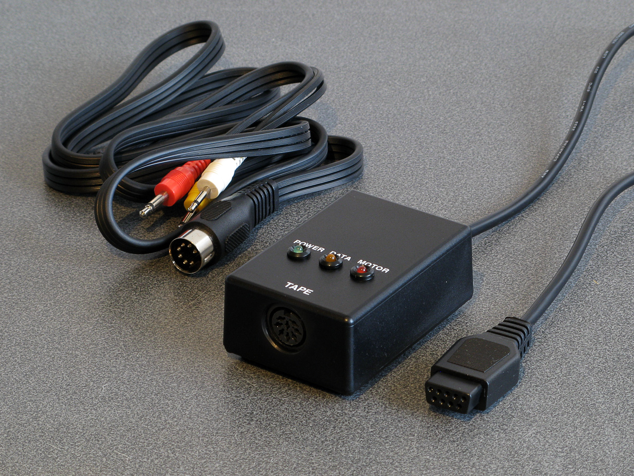
I have spotted two issues, though. The first affects my small cassette recorder but not the large one, and is related to reading files from tape via the file IO routines (such as OPENIN then BGET# to retrieve a single byte, not from LOAD). Files are stored on tape in 256 byte blocks, and when the file is opened a whole 256 byte block is read from the tape and copied to the Master System's RAM. When the BASIC program requests a byte from the tape it is read from this local copy of the block instead, and when the read pointer reaches the end of the 256 byte block the next block is fetched from the tape and the local copy updated with this new data. The motor control comes in handy here, with the file system library stopping and starting the tape playback as desired.
The problem I was having was that the first block would read fine, but when the time came to read the second block the tape started playing but the file system library never seemed to be able to detect any data – it would just work its way along to the end of the tape, never displaying any errors, but never reading any meaningful data either.
The issue ended up being some code I'd added somewhat recently to automatically calibrate the threshold between a 1200Hz ("zero" bit) and a 2400Hz ("one" bit) tone. The code reads bits by counting the length of each wave cycle and comparing this to a threshold value - if it's longer, it's the 1200Hz "zero" bit tone, if it's shorter, it's the 2400Hz "one" bit tone. Before and after each file, and between each block, is a section of 2400Hz "carrier" tone. By detecting a large number of wave cycles that were all around the same length (say, within four length units of each other) you could assume that you were receiving the 2400Hz carrier tone and use that to calculate a suitable threshold for loading in data later.
The main bug was that I was comparing the length of the wave cycle just received with the length of the previous wave cycle rather than the length of the first wave cycle. This becomes a problem when you start a tape that was paused in the middle of a carrier tone (e.g. between blocks) as the tape will take some time to come up to speed, during which time the period of each wave cycle will gradually decrease. As the reference length we're checking the current wave length against is changing over time it means we end up compensating for the tape's speed increasing and so end up accepting the slower (longer) wave cycle lengths as part of the calculation of the threshold between "zero" and "one" bit wave cycle lengths.
As the wave cycle length threshold is now longer than it should be, all incoming wave cycles get interpreted as short ones and so it looks like we're just getting a stream of "one" bits - which looks like the carrier, so the code never starts trying to decode any blocks. My larger tape recorder comes up to speed much more quickly than the small one, or at least doesn't audibly ramp up in speed, and so isn't affected by this problem.
Fortunately the fix is very easy, just check the length of wave cycles against the first wave received rather than the previous one. This way if the timings drift over time (as they would during the period that the tape is coming up to speed) then they'll eventually go out of the permitted range. Changing this fixed the issue.
You may wonder why I'm calculating the threshold at runtime instead of just using a hard-coded value if the expected frequencies are a fixed 1200Hz and 2400Hz. My main intention was to be able to handle tapes that were running at the wrong speed due to a miscalibrated cassette recorder, but this does also open up the possibility to load from tapes at higher rates. Without any further adjustment my code can already load from audio generated at 2320 baud, i.e. with the two frequencies at 2320Hz and 4640Hz, without any further adjustment. This is a slightly annoying figure as 2400 baud would be the obvious target (being double the intended rate!) but at this speed the current code fails to latch on to the signal so I slowed the "tape" speed down until I found a value that worked. It's perhaps worth mentioning that the audio in this case was coming from PlayUEF running on my phone rather than an analogue cassette tape with the BAUD (or LOW) parameter used to adjust the speed, I'm not sure that a 93% boost in loading speed would be achievable from a tape!
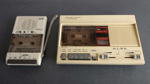
I mentioned above that there were two issues. The slow speed-up issue affected the small cassette recorder, but the large cassette recorder had a new issue that only became apparerent after moving the circuit to its final enclosure. The Master System should be able to start and stop the cassette remotely, handled by a reed relay that is then plugged into the cassette recorder's "remote" socket. The Master System was able to start both tape recorders without any issues, but was unable to stop the large one – the "motor" status light would switch off, but the tape would continue playing. Tapping the relay sharply would be the only way to get it to switch off.
I tried plugging in a 2.5mm TS plug into the side of the large tape recorder and used the very scientific approach of shorting its connections with a screwdriver to simulate the relay switching "on" and was surprised to see quite large sparks. I measured the DC current through the remote control switch when the cassette was running and it was only around 70mA at its highest – well below the 1A rating of the relay – however I reckon there is a very large inrush current when the motor kicks in that is sufficient to weld the reed switch contacts together, causing it to get stuck.
Why didn't this affect the circuit on the breadboard? In that setup I was using a 3.5mm TS extension cable connected to a 3.5mm male-to-male adaptor cable which was then connected to a 3.5mm to a 2.5mm adaptor cable. My assumption is that all of the extra contact resistances were helping to limit the inrush current, preventing the contacts from welding together.
It's very likely not the best sort of snubber circuit for this application but for the time being I've put a 10Ω resistor in series with the relay contacts, which limits the inrush current enough for the relay not to get stuck:
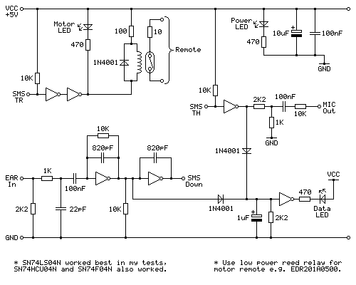
One matter that I've also been testing is the phase of the audio signal. As far as I can tell Acorn's tape format assumes a 180° phase; that is to say that each wave cycle starts at 180° and runs to 180°+360°=540° for a complete cycle rather than starting at 0° and running to 360°. The result of this is that instead of the signal starting at an amplitude of 0, then going positive before negative (as you'd expect for a typical sine wave) the signal goes negative first:
I have confirmed this by looking at the output of tools like PlayUEF as well as looking at the signals coming directly off commercially pre-recorded tapes with BBC Micro software on them, after first confirming that my sound card doesn't invert the signal by briefly connecting its input to a positive DC power supply and seeing that the received signal goes positive when that happens. Here's an example of a commercially-released tape, where you can see that after the high-frequency cycles in the first longer wave (a "zero" bit, acting as the start bit, starting at around 12.7065) starts low then goes high:
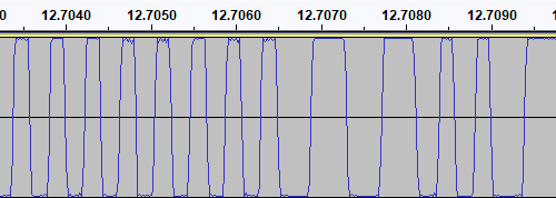
I then generated a test tone that alternates between 0 and 1 bits, i.e. one complete 1200Hz cycle then two complete 2400Hz cycles with the appropriate 180° phase:
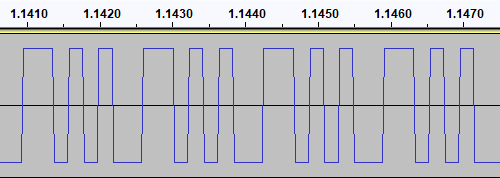
This pattern should make it easy to spot the phase of recordings. I first tried running the test tone straight back into my PC to ensure that the phase was not being reversed by the PC, and got the same signal back in compared to to what I played out, as you'd expect. I then tried recording the signal to tape with my Grundig recorder, and found something interesting when playing it back:
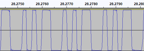
The phase there is very clearly reversed – the signal I played into the tape recorder goes low before it goes high, whereas the signal I've recovered goes high before it goes low. I repeated the test with the Alba tape recorder:
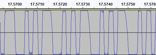
This shows the same thing – the phase on the tape is at 0° even though the test signal was at 180°. I also have a Sony digital voice recorder (an ICD-BX140) that I've been using as well as a tape recorder, so I tried the test with that too:
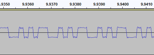
Apart from the much lower recording level this once again shows the same thing – the signal phase is inverted when recorded.
I had previously encountered an issue where I had tried to make a tape from a UEF image by playing the audio generated by PlayUEF into a tape recorder. Attempting to load the data directly from PlayUEF worked fine, but the tape recording of the same signal wouldn't load. My Grundig tape recorder has a phase reversal switch, and setting it to "reverse" would allow me to load the tape created by recording the output of PlayUEF. However, in that reverse setting, I lost the ability to load from my commercially-recorded tapes. I think the above tests indicate why this is the case – the recorders all invert the signal when creating the tape recording. I find it particularly interesting that the Sony digital voice recorder does the same thing!
I did check to see if the phase switch on the Grundig tape recorder had any influence on the recording, but it doesn't – whether it's set to "normal" or "reverse" the recording to tape still ends up inverted. The phase switch only appears to affect playback.
PlayUEF does have an option to set the output phase to 0° instead of its default 180°. By doing that and recording its output to tape I was able to load the programs directly from either of my tape recorders.
Of course, it would be nice if the loader was able to handle either phase, and in practice I've found it does sometimes handle the "incorrect" phase quite well but it does seem to be more a lot more error prone – some programs load without any problem, others report problems with some blocks and others fail to be detected at all! I think I'll see if there's a way to reliably detect the phase and switch to the appropriate handler, but for the time being I've added a crude workaround – pulling pin 1 of the controller port (the d-pad "Up" input) to ground tells the loader to assume the phase is inverted. As I hope this won't be necessary in future I've left this as a jumper in my current tape interface circuit (visible below in the top left corner) rather than add a switch!
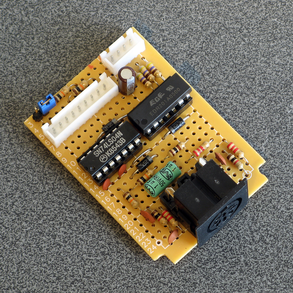
A lot of the work has been focused on the tape loader, but tapes are not the most practical storage media these days. Finding a working tape recorder is a challenge in its own right, and a lot of the old tapes are tricky to work with as they've become sticky with age. In an attempt to be a bit more modern I've started integrating support for the VDrive3 to BBC BASIC. This is an inexpensive module that lets you access files on a USB mass storage device via simple commands sent over a serial interface. I'd previously used the VMusic2 device in another project and that uses the same firmware commands so I already had a little experience with it (the VMusic is pretty much a VDrive with an MP3 decoder bolted on top). I already had some serial routines written so it was a reasonably easy job to plumb in some code to handle LOADing and SAVEing programs, and from a hardware perspective all you need is a cable to connect the module directly to the Master System's controller port – the VDrive3 uses 3.3V signalling levels but its I/O lines are 5V tolerant.
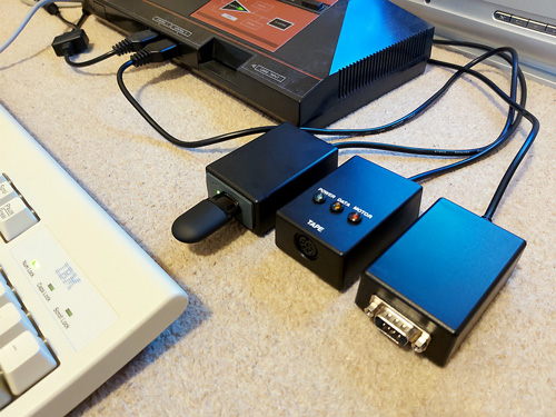
One notable advantage of the VDrive3 over the tape interface is that it allows for proper random-access of files rather than just sequential access. I've been working on implementing all of the required BASIC statements to support this (OPENIN, OPENOUT, OPENUP, BGET#, BPUT#, PTR#, EXT#, EOF#, CLOSE# etc). For a bit of fun I wrote a BASIC program that loads an image file from disk (or tape) and displays it on screen. I needed to add user-defined character support to the new reduced-resolution MODE 2 to handle this (something that was not implemented before due to a lack of VRAM) but with that in place it's working pretty well.
It's not fast, taking 2m45s to load from from tape and 1m19s from a USB flash drive, but it's a fun diversion!
Refining the tape interface for BBC BASIC on the Sega Master System
Tuesday, 28th September 2021
It's been quite a while since my last post but work has continued with the version of BBC BASIC (Z80) for the Sega Master System. Most of the features I have been working have not been particularly exciting to write about on their own, but here are some of the notable changes:
- All VDU code (for text and graphics output) has been moved to a separate ROM bank, freeing up around 16KB of extra ROM space. It makes calling the code slightly more complicated but in the previous post I mentioned that I had less than 100 bytes of free ROM space so this was definitely required.
- Simplified the video mode driver interface. Each video mode has its own driver code which exposes a number of different functions. Previously, each function had its own vector in RAM which was fast but consumed a lot of precious work RAM. Now only a couple of functions (which need to be called frequently and as quickly as possible) are vectored, and all of the other functions are called via a single generic function with a parameter for which specific operation to carry out (e.g. "reset the graphics viewport", "change the text colour").
- Rewrote the triangle filling routine and line drawing routine to ensure that the same pixels are covered whether you fill a triangle or trace its outline – previously there would be some stray pixels that leaked outside the perimeter of a filled triangle.
- Changed the output resolution for most video modes to 240×192 with a logical to physical pixel scale factor of 5⅓ for a total logical resolution of 1280×1024, the same as the BBC Micro – graphics programs designed for the BBC Micro now properly fit on the screen.
- Changed MODE 2 to use a smaller resolution of 160×128 with a pixel scale factor of 8. Unfortunately, there is not enough video RAM to have a unique pattern in VRAM for every character position on-screen when using all 16 colours (as in mode 2) at the higher 240×192 resolution. The new lower resolution avoids screen corruption that previously occurred when running out of VRAM:


MODE 2 graphics at the full-screen 240×192 and reduced 160×128 resolutions
- Added support for scrolling the text viewport down as well as up, this is used by the line editor which now allows very long lines to be edited in small viewports by scrolling and repainting as necessary.
- Reworked the keyboard input routines for greater reliability and performance, including proper mapping of key codes in *FX 4,1 and *FX 4,2 and removal of "clever" (but flawed) interrupt-based detection of when a key is available (that had a habit of dropping keys and resulted in worse performance than just periodically polling the keyboard anyway).
The most significant changes have been all to do with loading and saving from tape, though. Since my previous post I have been doing a lot of work testing and refining both the hardware and software of the tape cassette interface. The hardware has now been tested with a couple of different tape recorders, as well as a pocket digital recorder, my mobile phone and my PC's sound card. The loader is much more robust and if a single block fails to load from the tape you can usually just rewind the tape a short way and it will try again, no need to rewind back to the start and start from scratch. I was previously counting the duration of half-wave cycles from the tape and comparing these to some fixed thresholds baked into the code to determine the difference between a "0" and a "1", I've now changed this to measure full-wave cycles (which aren't affected by any duty-cycle shifts in the recordings) and to calibrate the thresholds during the initial carrier tone, which allows the code to compensate for tape recorders that aren't quite running at the correct speed. On a more practical basis I've also added the ability to save to tape, motor control via a reed relay (so the tape will automatically stop after a file is loaded), and support for opening files on tape for reading or writing and accessing them on a byte-by-byte basis. As tapes are sequential access there are some limitations to this (for example, you can only advance the read pointer later in the file, you can't seek backwards) but it works quite well otherwise.
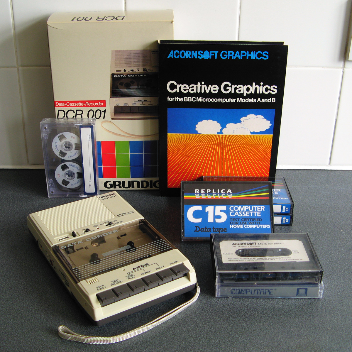
Of course, to test all of this I needed a tape recorder! I purchased the above Grundig DCR 001 data cassette recorder as well as some blank cassettes and a couple of commercially-prerecorded ones to do so. The DCR 001 has a few nice features that make it great for loading programs:
- A dedicated "data" mode that sets the output level at an appropriate fixed level – no need to guess about finding a suitable volume level.
- An optional "monitor" in data mode that lets you listen to the data on the tape as it's loading.
- A "phase" switch that can be used to reverse the phase output, to compensate for the case where the data has been recorded with a 180° phase shift.
- An "Automatic Programme Detecting System" that lets you skip ahead to the next program or back to the previous one by pressing Rewind or Fast Forward when Play is pressed – this stops when it detects a silent gap between recorded sections of data on the tape.
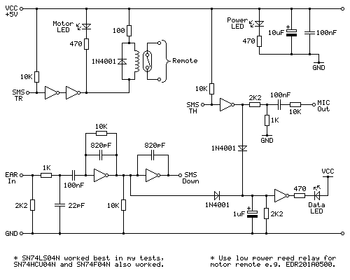
Above is the cassette interface circuit I came up with. It's quite simple and has a notable lack of analogue sections (no op-amp chips here!) – it uses a NOT gate with a 10KΩ negative feedback resistor to turn the analogue signal from the tape recorder's earphone output into a clean digital signal that can be fed into the Sega Master System. I've tested this with an SN74LS04N, SN74HCU04N and SN74F04N and all worked well, however for best results I'd recommend the SN74LS04N. The filtering capacitors clean up some high-frequency pulses/glitches that may otherwise end up on the output; this is not something I found was much of a problem with a cassette recorder or the audio output from my phone or PC, but a pocket digital voice recorder I have seems to produce glitchy high-frequency pulses in its output (I'm not sure if that's an artefact of its DAC or in the MP3 compression it uses for its voice clips) and those capacitors clean up the signal enough to be able to read it reliably.
The remote motor control relay is a reed relay, and must be a low current device to avoid overloading the Master System's controller power supply and to also allow it to be driven directly by the hex inverter chip. I found the EDR201A0500 perfect for this role!
Being able to save and load back programs on one cassette recorder is fair enough, but to really be sure my hardware and software are working as they should I thought I should see if I was able to save a program to tape on one tape recorder and then load the same program back on a different tape recorder. To this end I bought the above cassette recorder. It was clear from the listing that the record button and counter reset button were damaged, and the whole thing was quite grubby, but I thought it worth a punt.
Getting inside was very easy as all but one of the screws was missing, and it was clear that someone had got there before me as the damaged plastic parts (including two of the main screw posts as well as the snapped-off parts of the record button and counter reset mechanism) had been removed at some point. After giving the tape path a very thorough clean and replacing one of the drive belts that was turning into a tarry mess I was able to get it to play a tape, so I took everything out of the enclosure to give that a good scrub and prepared to fix the damaged plastic parts.
By tracing the arm from one of the other buttons onto a piece of scrap ABS plastic I was able to make a replacement arm for the damaged record button, which I then glued on with cyanoacrylate and some two-part epoxy resin to fill in the gaps. The result is not especially pretty but it does the job and my blobby repair is not going to be visible unless you take the recorder apart.

The counter reset button was a bit more fiddly; the reset mechanism seems to rely on the "n" shaped bit of plastic shown above in the top left photo, and though it looked like something used to be attached to it that had snapped off I wasn't sure what it would have originally looked like. I cut up some more scraps of ABS sheet to make up a new counter reset button which seems to work pretty well, though!

The final addition was a couple of new knobs for the tone and volume sliders – these are cheap generic parts and they don't quite line up with the markings (the original sliders have off-centre indicators) but overall I think this turned out pretty well, and my main concern – being able to save a program to tape on one machine and then load it back from another – has been thoroughly tested now and I'm happy with the results. My next task is to transplant the circuit from its current breadboard layout to a neat project box!
Better drawing, editing, memory and emulation for BBC BASIC on the Sega Master System
Tuesday, 3rd August 2021
I have continued to work on the Sega Master System version of BBC BASIC, and it's feeling much more like a practical version of BASIC than something that was just holding together to run one specific program!
One of the key improvements is to standardise the handling of the different graphics modes. Previously I was using a coordinate system where (0,0) is in the top left corner and all drawing operations were carried out using physical device coordinates (so the screen was treated as being 256 pixels wide and 192 pixels tall). I have now moved the origin (0,0) into the bottom left corner with the Y axis pointing up and scale down all coordinates by 5, effectively making the screen 1280 logical units wide and 960 units tall. This isn't 100% compliant, as the BBC Micro and other versions of BASIC treat the screen as being 1024 units tall, but dividing by 5⅓ is considerably trickier and it would result in the graphics being squished further vertically, so I think using a logical resolution of 1280×960 is an acceptable compromise. I've added some VDU statements to allow you to move the graphics origin as well as define custom graphics and text viewports, so you can control where on the screen graphics and text appear and how they are clipped/scroll.

The output of the "Mandelbaum" program following these changes
I have also changed the default palette to more closely match the one used by the BBC Micro and other versions of BBC BASIC. This isn't too difficult when using the Master System's "Mode 4" as that has a user-definable palette, but the legacy TMS9918A modes have a fixed palette so I've tried to match the default palette as sensibly as I can to the TMS9918A palette. It's possible to change the logical to physical palette mappings under Master System "Mode 4" via a VDU command which writes directly to the CRAM (you can either remap one of the 16 logical entries to one of the stock 16 colours, or supply an RGB value directy to select additional colours) which allows for neat tricks like palette cycling, but the TMS9918A modes currently only let you change the current text/drawing colour, not amend the palette as that's fixed in hardware.
I've also added filled/outlined circle and axis-aligned ellipse PLOT commands using some code written by Darren "qarnos" Cubitt which I originally used in the TI-83 Plus version of BBC BASIC. This code is very capable and fully accepted 16-bit coordinates for its inputs, however it was also originally designed to output to a 96×64 pixel screen so the final plotting was done with 8-bit coordinates ranging from -128..127. Fortunately the Master System's screen also fits in 8-bit coordinates at 256 pixels wide but that's not quite enough information as you also need to be able to tell if a particular point is off-screen (less than zero or greater than 255); simply clipping it against those boundaries will result in a vertical smear on the left or right edge of the screen when drawing outlines. Fortunately I was able to figure out how to modify his code to add some extra clipping status flags to ensure that ellipses were clipped and displayed correctly on any part of the screen.


Filled circles and filled/outlined ellipses make these drawings possible
The only graphics operation exposed by the mode-specific drivers before was a simple "set pixel" routine. This is fine for lines but quite slow for filling shapes so graphics mode drivers can now supply a "fill horizontal span" routine for faster shape-filling. If the routine is left unimplemented a stub routine is provided that fills the span using the "set pixel" routine.
I also added a rectangle-filling PLOT command, which is perhaps not the most exciting-sounding graphics operation but it is used to clear the screen so it is at least useful. More interesting is a triangle-filling routine, something I've never enjoyed writing!
Usually I get very bogged down in the idea that the pixels affected when you fill a triangle should exactly fit within the pixels that are outlined by drawing lines between each of the triangle's points, no more and no less. This can be a bit difficult when the triangle is filled by tracing its edges from top to bottom and drawing horizontal spans between them. If the edge is "steep" (its overall height is greater than or equal to its width) then this isn't too bad, as there's only one X coordinate for each Y coordinate where a pixel would have been plotted. However, when the edge is "shallow" (its overall width is greater than its width) there are going to be certain Y coordinates where the line drawn would have had multiple pixels plotted. In that case, where is the boundary of the horizontal span?
The cop-out answer I've used in the past has been to set up three buffers the total height of the screen and to "draw" the three lines first using the same line-drawing algorithm as the line PLOTting command, keeping track of the minimum and maximum X coordinate for each Y coordinate. When it's time to fill the triangle the minimum and maximum X coordinate for each edge can be determined based on the current Y coordinate and a span drawn between them for perfect triangles. On the TI-83 Plus this takes up four bytes per line (minimum and maximum 16-bit values) for a 64 pixel tall screen, with three buffers for the three lines that comes to 4×64×3=768 bytes, pretty bad. On the Sega Master System that would be 4×192×3=2304 bytes, totally unacceptable on a machine with only 8KB total work RAM!

Each face of this 3D sphere is filled by two triangles.
I've instead simply done my best to interpolate from one X coordinate to the other when working my way down the triangle and filling scanlines, doing a bit of extra pre-incrementing and fudging of initial error values depending on whether it's the top half or bottom half of the triangle. My test was to draw the outline of a triangle in bright white and then to fill a dark blue triangle over the top, if any bright white pixels were visible around the outside this indicated a gap. I mostly got it filled, but I then tried my test program on a BBC Micro emulator and found the BBC Micro exhibited similar gaps so I don't think I'm doing too badly! The above screenshot of the 3D sphere was rendered using this triangle-filling code.
I've also been working on improving the line editor. This is called by BASIC when it's asking for a line of text input from you. Previously I'd only implemented adding characters to the end of the line and pressing backspace to remove characters from the end of the line; if you'd typed in a long piece of code and made a mistake at the start you'd need to backspace all the way to the mistake, correct it, then re-type the rest of the line. Now you can use the cursor keys (or home/end) to move around within the line, insert or overwrite new characters (toggled by pressing the insert key on the keyboard) at the cursor position or backspace/delete characters mid-line as required. It sounds like a small thing but it was quite a lot of code to get right and makes a big difference for usability!
Another feature I've added to aid modifying lines of code is the *EDIT command. This takes a line number as an argument and then brings up the program line you've requested in the line editor, ready for editing. The way this works is a bit sneaky, as it's not natively implemented by BBC BASIC! The trick that makes it work is the ability to override two routines, OSLINE (which BASIC calls when it wants to display the line editor) and OSWRCH (which BASIC calls when it wants to output a character).
When a valid *EDIT <line> command is entered, OSLINE is overridden with the first custom routine. This routine doesn't ask for a line of input, but instead copies L.<line> to the input buffer, overrides OSWRCH with a routine that captures data to RAM, overrides OSLINE with a second custom routine, then returns. BASIC therefore thinks you've typed in a LIST statement so it dutifully starts outputting the line via OSWRCH, but this has been overridden to write the characters to RAM rather than the screen. When it's done this BASIC then calls OSLINE again for the next line of input, which brings up the second custom OSLINE handler. This pulls the data from RAM previously captured by the OSWRCH handler, copies it to the OSLINE buffer, and dispays it on-screen as if you'd just typed it in. It then restores the original OSLINE and OSWRCH handlers before jumping back into the stock OSLINE routine, so you can continue editing the line that you'd requested via *EDIT.
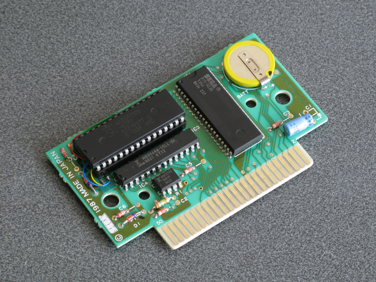
All of this hopefully makes entering programs via the keyboard less cumbersome. Of course, not having to type in programs in full every time you wanted to run them would be even better, and an attempt to give BASIC more memory provides another way to load programs in a somewhat roundabout manner.
The photograph above shows the modified Monopoly cartridge that I'm now using to test BBC BASIC on real hardware instead of the modified After Burner cartridge I was using before. The advantage of Monopoly is that it has an additional 8KB RAM on board, which is used to save games in progress. Sega's cartridge mapper allows for on-cartridge RAM to be mapped into the address range $8000..$BFFF, immediately below the main work RAM which is at $C000..$DFFF. If present, then, BASIC's memory range (which runs from PAGE to HIMEM) can be extended by enabling the save RAM and moving PAGE down.
$8000..$BFFF is a 16KB range, though, and I mentioned that Monopoly has an 8KB RAM. This is true, and what it means is that the 8KB cartridge RAM is accessible from $8000..$9FFF but is then repeated ("mirrored") from $A000..$BFFF. The cartridge RAM detection therefore has to check two things: firstly that there is RAM in the first place (which can be verified by modifying memory at $8000 and seeing if those values stick) and how big it is (which can be checked by writing to $8000 and seeing if that has also modified the data at $8000+<RAM size>). Once presence of any RAM has been determined during startup, RAM mirroring is checked in 1KB, 2KB, 4KB and 8KB offsets. If any RAM mirroring is detected, then it's assumed the RAM is the size that was being checked at the time, however if not it's assumed that the RAM is the full 16KB. At this point, PAGE (which is $C000 in a stock machine with no cartridge RAM) is moved backwards by the size of the detected cartridge RAM, e.g. to $A000 for an 8KB RAM and $8000 for a 16KB RAM. This results in 16KB or 24KB total available to BBC BASIC, a considerable upgrade from the plain 8KB work RAM!
An added bonus of this is that when you type in programs they grow upwards in memory from PAGE. As PAGE now starts within your cartridge memory, and that cartridge memory retains its contents courtesy of a backup battery, it means that if your entered program is smaller than the size of your cartridge memory you can restore it when you switch the console back on by typing OLD.
That's very well for life on real hardware, but I continue to do most of my development testing in an emulator. I'm having to use my own emulator as there aren't any other Master System emulators that also include a PS/2 keyboard emulator, but I did end up running into a very weird bug. Certain trigonometric functions in BBC BASIC were producing very wrong values, resulting in very odd-looking output.


These shapes are on the wonk
Even though the Z80 emulator at the heart of the program passed ZEXDOC (an instruction tester that checks documented functionality) I remembered that it had failed some aspect of ZEXALL which checks the undocumented flags too. I re-ran ZEXALL and found the problem was with my implementation of the bit instruction, so I worked on fixing that including emulation of the Z80's internal temporary memptr/WZ register to ensure that bit n,(hl) set bits 3 and 5 of the flag register appropriately. ZEXALL now passes, but unsurprisingly it didn't fix my problem (as I didn't really think that BBC BASIC would rely on undocumented functionality!)
I ended up isolating certain exact values that when plugged into SIN() or COS() would produce incorrect results. I then dug out my old CP/M emulator and tried plugging those values into the generic CP/M version of BBC BASIC (which has none of my code in it!) and that produced the same, incorrect, results confirming that the issue was definitely in my Z80 emulation and not in some flaw of the BBC BASIC port.
After tracing through the code and dumping out debug values at certain points and seeing where it differed to a known good reference emulator I found that the fault occurred in FMUL, and from there I found that at some point the carry flag (which is either rotated or added to registers with RR or ADC instructions) was being lost. RR looked fine but digging into my implementation for the 16-bit ADC I found the culprit: the code is the same for ADD and ADC, but in ADC if the carry flag is set then the second operand is incremented by one first. This produces the correct numeric answer, but if the second operand was $FFFF on entry to the function then adding a carry of 1 to it would cause it to overflow back to 0. As this happens before any of the rest of the calculations are made it means that the final value of the carry flag was calculated based on op1+0 instead of op1+$10000, hence the loss of the carry flag.
Fortunately, fixing this fixed the wonky output demonstrated above and I feel slightly more confident in my emulation! Now I can continue working on BBC BASIC, I've had an idea for a screen mode that has a reduced number of colours but will hopefully let you draw anywhere on the screen without running out of tiles causing odd corruption (as happens in the usual 16-colour mode 4) and without attribute clash (as happens in the TMS9918A Graphics II mode)...
Running BBC BASIC on the Sega Master System
Thursday, 22nd July 2021
I've recently been spending some time finding a way to run BBC BASIC on the Sega Master System, inspired by BASIC Month 6: The Mandelbaum Set on the RetroBattlestations Reddit community.

When this month's program was first announced I tried running it on my only unarguably retrobattlestation, my Cambridge Z88, but the screen's low (vertical) resolution didn't do the program much justice.
I thought this gave me two options:
- Control some external piece of retro tech to produce higher-resolution output (e.g. a printer or a plotter.
- Port a BASIC interpreter to another retro system with a higher resolution display and run the program on that.
Unfortunately, I don't own any old printers or plotters (or a Logo-like turtle!) so option 2 seemed my best option. I had some experience adapting Richard Russell's BBC BASIC (Z80) to run on the TI-83 Plus calculator so I thought I should pick the Sega Master System as that also has a Z80 CPU in it. Here are some rough specs:
- 3.58(ish)MHz Z80 CPU.
- 8KB work RAM.
- TMS9918A-derived VDP for video with 16KB dedicated VRAM accessed via I/O port.
- SN76489-derived PSG for sound.
- Two controller ports with six input pins and two pins that could be configured as inputs or outputs.
- Software loaded from ROM cartridge or card slot with a small BIOS ROM that detects whether a cartridge or card is inserted (and if not, runs its own built-in game).
There is some precedence to this endeavour with the computer version of Sega's SG-1000, the SC-3000, which came with a keyboard and had BASIC ROM cartridges.
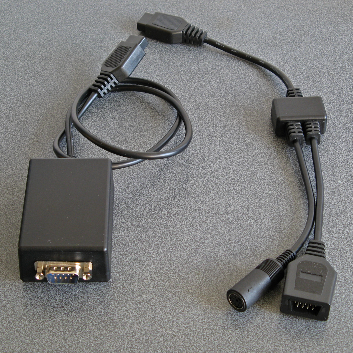
I wanted to try to keep this project as retro as possible, so no modern microcontrollers as I've been accused of cheating by using them in the past. I did have to make a couple of adaptors to allow me to plug in a keyboard and to give the Master System a serial port to load or save programs over – more about these later!
Loading BASIC onto the Master System
The first problem was getting BASIC onto the Master System at all. As my Master System doesn't have BASIC in ROM (it comes with Hang-On, which is perhaps more fun but less likely to handle the Mandelbaum set) I'd need to load the program onto a cartridge or card. Master System cartridges usually contain a mapper circuit to handle bank switching in the lower 48KB of the Z80's address space (the upper 16KB contains the 8KB work RAM, appearing twice) which is normally integrated directly into the ROM chip for the game, however there are a handful of games that have separate mapper chips and ROM chips and the ROM chips that Sega used have a pinout that is extremely close to that used by common EEPROMs (e.g. 29F010,
49F040) with only a couple of pins needing to be swapped around. After Burner is one such cartridge, so I've modified an old copy to let me plug in flash memory chips that I can program with the version of BASIC I'm working on. A switch at the top of the cartridge lets me switch back to the original pin configuration if I want to play the original copy of After Burner.
Typing commands into BASIC
With a flashable cartridge to hand I was able to assemble a version of Richard Russell's BBC BASIC (Z80) with some simple code stubs in place to direct text output to the screen. Output is useful but only half the story, we still need to be send commands to BASIC!
The Master System doesn't have its own keyboard, so I'd need to find some way to interface one to it. I have previously used PS/2 keyboards in a number of projects, as they are pretty simple to deal with. Electrically, they use two open collector I/O lines for bidirectional data transfer (one as clock, one as data), and fortunately each controller port of the Master System has two pins that can be configured as outputs which can therefore be used to interface with a keyboard (either left as inputs and pulled weakly high in their idle state, or driven low as outputs for their active state).

It acts as a pass-through cable so you can still have a regular controller plugged in when using the keyboard.
The two pins on the Master System control port that can act as outputs are TH and TR; TH is normally used by light guns to latch the horizontal counter in the video chip so is unused with normal controllers so it's no great loss here, but TR is the right action button (marked "2") so by using this pass-through adaptor you do unfortunately lose one of the controller buttons. However, you do gain a hundred or so keyboard keys, so I don't think it's too bad a compromise...
For the software side of things I adapted my Emerson AT device library, previously written for the TI-83 Plus calculators, to the Sega Master System hardware. This library handles the low-level AT device protocol and also translates the raw keyboard scancode values to the corresponding characters.
Saving and loading programs
At this point I was able to type in BASIC programs and run them on the Master System, which was pretty neat! However, I was still working on adding new features (e.g. drawing commands for graphics) and having to type in the entire Mandelbaum program after every change was going to get pretty exhausting. I could bake it into the ROM but that seemed like cheating, so I thought I should try to find a way to load the file from an external source. A floppy disk or tape cassette would seem authentically retro but adding a floppy drive controller to the Master System would be a fairly complicated task and I don't have a suitable data cassette recorder to even attempt loading from tape so I thought some sort of file store accessible over a serial port would be a good option.
The Z88 has a serial port and can act as a remotely-controlled file store when running the PC Link software (with the protocol documented here. This seemed like a good choice, if not for the fact that the Sega Master System doesn't have a serial port of its own. To get around this, I added one, using a MAX232 chip to adapt the Master System's 5V logic levels to RS-232 compatible ones so I could plug in a null modem cable from the Z88 or my PC without accidentally frying the Master System with -12V.
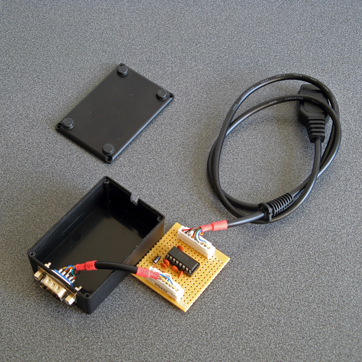
I wrote some code that bit-bangs the serial data over the controller port lines using the timing loop code I wrote for a previous BASIC Month (Crisps Tunes) to support rates between 19200 and 300 baud. 19200 baud is somewhat unreliable but that's OK because the Z88's 19200 baud is unreliable too, so the default 9600 baud speed does a good job. RTS/CTS handshaking has to be implemented, as there is no hardware serial support on the Master System and it needs to be actively polling the port to receive any data. In doing so I noticed one awkward fact about my PC's serial port - if you de-assert RTS it will continue sending data until its buffer is empty, presumably only checking the RTS line when it's about to top up the buffer. In practice this means that even if I change RTS virtually as soon as the start bit for the first byte is received, the PC will continue to send up to 256 bytes before stopping. To get around this I added a serial receive buffer that immediately checks for the next byte even after asserting RTS, and this seems to have done the trick.
The protocol used by PC Link requires acknowledgement after every single byte so is very slow but at least it's reliable. I plumbed the PC Link code into BASIC's LOAD and SAVE which makes loading and saving programs as transparent and easy as if you had a floppy disk in the system instead!
Pressed for size
The Master System has 8KB of RAM. Of this, 16 bytes are mapped to special hardware functions and BBC BASIC reserves 768 bytes for itself, so we're already down to 7,408 bytes. I initially reserved 256 bytes for my own needs (display settings, VDU command buffer, serial port status, keyboard status etc) bringing it down to 7,152 bytes. The 16KB of display memory is not directly accessible to the CPU, so it can't be used for additional work RAM, and having to access it indirectly via I/O ports is very slow but I can't afford to mirror parts of it in RAM for speed.
Initially the Mandelbaum program ran well enough by stripping out comments, but I then added sound support (with eight 13-byte envelope definitions, and four channels with their own state, copy of their active envelope and a command queue for 32 bytes per channel, adding around another 140 bytes of memory usage) and the program stopped running with a "No room" error during execution (performing a square root operation, of all things!) so I guess the tolerances were very tight. I went and combine more lines of code into single lines and replaced two-letter variable names with single-letter ones (no, really) and it was able to run again but I don't think 8KB is a particularly comfortable amount of RAM for a BASIC computer!
Further design considerations
The version of the BASIC host interface used here is very much a work-in-progress. I would need to extend it considerably to be useful, including:
- Fuller support of different VDU commands, e.g. redefining character shapes, changing the text and graphics viewports, better colour handling (differentiating between logical palettes and physical palettes).
- Better support of other modes (so far only TMS9918A "Text" and "Graphics II" modes are used, there is a Master System-specific "mode 4" but that lacks graphics support and only takes advantage of hardware scrolling for extremely fast program LISTing).
- Implementation of more graphics commands - so far only PLOT 4 (MOVE) and PLOT 5 (DRAW) are implemented. They also use a non-standard coordinate system with (0,0) in the top left of the screen and a screen resolution of 256x192, whereas for standardisation with other BBC BASIC implementations this should move (0,0) to the bottom left and use a logical resolution of 1280x1024 or similar.
- Support of other file systems rather than rely on a Z88 running PC Link, e.g. using I²C EEPROMs (as they use two open collector pins, so could be plugged into a controller port via a passive adaptor).
- Support of extra RAM, either integrated directly on a custom cartridge or using the battery-backed SRAM supported by some other cartridge types.
- Native controller support via BASIC ADVAL command (at the moment you can access the controller ports directly with GET(&DC))
This is before even getting into adding anything machine-specific (e.g. to take advantage of scrolling tilemaps or hardware sprites), but getting the BASICs down (and consistent!) is a very important starting point. Consistency is useful, after all I was able to get the original program running under BBC BASIC with very minimal changes to it.
But, in the short term, I have at least succeeded in what I set out to do, which was to run the Mandelbaum program on a retro "computer" wholly unsuited to it!

The above video provides another demonstration of the setup – playing the Cold Tea music demo, albeit with a heavily stripped-down version of the visuals as the Master System doesn't have anything that can match the capabilities of the BBC Micro's teletext mode 7.
Making your own Dreamcast MIDI Interface Cable
Saturday, 1st May 2021
I love an unusual accessory for a video game console or computer, and one such accessory is the Dreamcast MIDI Interface Cable, HKT-9200, which allows you to connect MIDI devices to the Dreamcast console's serial port. Only released in Japan and with only one piece of software released for it — the O・to・i・re (お・と・い・れ) sequencer – these are a somewhat hard to find accessory nowadays and prices for second-hand units are far beyond what I could hope to afford (at the time of writing there are two on eBay, both for over £300).
Fortunately, the user darcagn on the Obscure Gamers forum took some photos of the insides of the interface box and from that I could make a pretty good guess as to how the cable works.
MIDI uses a serial protocol running at 31.25Kbps (a speed that can be easily derived by dividing a 1MHz clock by 32). Rather than signal "0" or "1" bits with different voltage levels (as with a PC's RS-232 serial ports, for example, which commonly uses +12V for a "0" and -12V for a "1") it uses a current loop, with 5mA current on for a "0" and current switched off for a "1". To avoid ground loops, which are a big concern when working with audio as they can introduce intereference (e.g. a mains hum) on recordings, the two connected devices are electrically isolated with an optoisolator in the receiver.
At the very least I therefore expected to see some sort of optoisolator circuit on the adaptor's MIDI IN port and some sort of output buffer circuit on the adaptor's MIDI OUT port to convert between MIDI's current loop signalling and the Dreamcast's 3.3V logic on its serial I/O pins, and that is indeed what you can see from darcagn's photos. My worry was that there might be some additional Dreamcast-specific hardware inside the box, but fortunately there isn't – it's all off-the-shelf parts. My main concern was how everything was connected, as this can't be completely seen from the photos: would sending MIDI IN data to the console's serial port RX and relaying data from the console's serial port TX to MIDI OUT be enough? Some experimentation would be necessary!
Building a serial port connector
As mentioned above, the MIDI interface cable's box doesn't contain anything Dreamcast-specific, however this box is connected to the Dreamcast's serial port using a proprietary connector. To try anything out I'd need to find a way to connect a circuit to this port:
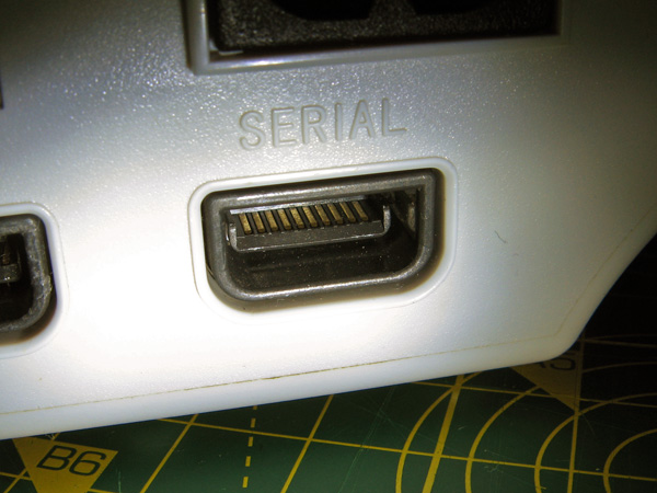
Fortunately, the port's contact pitch is the same as a PCI Express slot, and I was able to find a PCI Express slot for £5 which could be used to make multiple connectors! It will need to be cut down to size (and in half, as the Dreamcast's serial port only has contacts on one side rather than both sides of a PCI Express card) but with a bit of work will do the job.
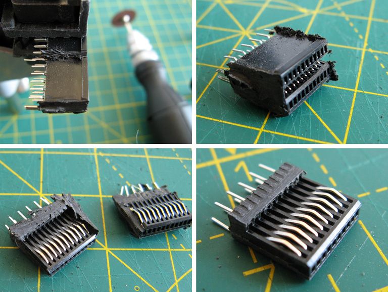
The above photos show the process of cutting the PCI Express slot down to size. The Dreamcast serial port has 10 connectors in it, so a block is cut that is 12 connectors long using a cutting disc – as this is quite a rough process an extra sacrificial connector is left on each end as it doesn't matter if this gets mangled by the cutter. The block is then cut in half, leaving more of the support structure from the bottom of the slot on the side of the slot we're going to be using. The outer two connectors are then removed if they haven't already been damaged, leaving the central 10 connectors, and the outer plastic is brought to the final width and tidied up with some hand files. The fit of the connector should be tested against the Dreamcast's serial port:
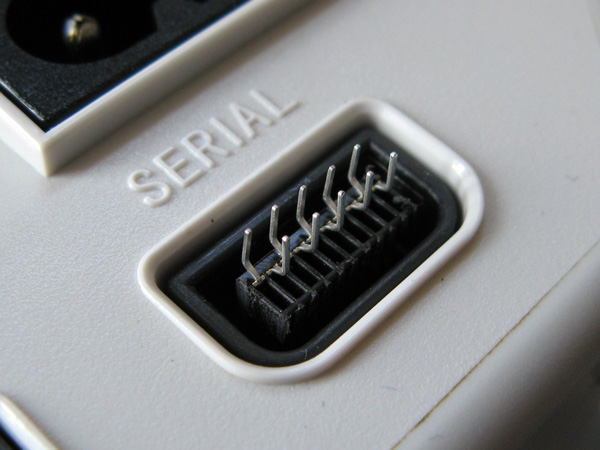
There shouldn't be too much side-to-side movement but the connector will be very loose without something to hold it down against the contacts. In my case I found some 2mm thick ABS plastic sheet was the perfect material to make the backing piece for the connector, though you may find your choice of material depends on the thickness of your PCI Express slot. It will need to be 13.5mm wide (about ½") and a decent enough length to fit inside the enclosure you're going to use for the plug – in my case 4cms was about right. The plastic can be cut by scoring it with a knife and then snapping it over the edge of a table.
You should also drill some shallow holes in the plastic, with the centres of the holes being 3mm from the end and 3mm from the sides. The serial port has a couple of bumps stamped into the metal surround of the serial port and these matching holes in the plastic piece allow it to snap into place. A stripboard track-cutting drill is perfect for this task!
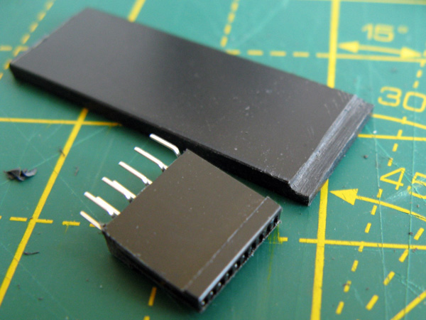
In my case the PCI Express slot also has a slight lip that prevents it from sitting flush against the backing support. I could have filed this flat but the connector is quite fragile so I didn't want to risk damaging it so I ended up filing a corresponding channel into the bottom of the backing support piece.
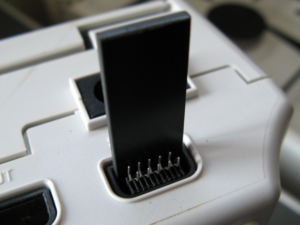
At this point make sure that everything fits. If it does you can start wiring up! The photos below show the process – heat-shrink tubing and strain reliefs are very useful, so don't forget to install them before soldering!
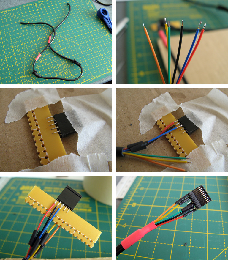
Putting a scrap piece of circuit board material between the two rows of pins also makes soldering much easier. In my case I only soldered the six pins required for this MIDI interface cable:
- 1: +5V
- 3: GND
- 4: RX
- 5: TX
- 8: GND
- 10: +3.3V
Pins are numbered from left to right when looking at the serial port at the rear of the console (if in doubt, you can check the voltages of the end pins against the console's metal chassis ground).
At this point you may wish to double check that your solder connections are made correctly and that nothing is shorted out – try with the cable plugged into the Dreamcast as well, and check that adjacent pins are not shorted together (the only two that should be shorted are pins 3 and 8, the two GNDs). If you're happy with that you can glue the connector onto the backing:
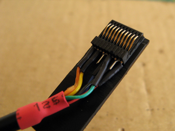
You may notice that this is actually a different connector in the photo to the previous one, and that's because I accidentally got glue into the connector's springy contacts and jammed them so had to start again – definitely not a fun mistake to make, so be careful!
Fortunately, the second one went more successfully. The glued connector snaps in and out of the console with a nice reassuring click thanks to the two holes drilled into the top surface. Before switching on the Dreamcast I tried wiggling the cable around to ensure that even when treated roughly it woudn't short out adjacent pins. When I was happy this was the case I switched on the Dreamcast and ensured that I was getting a consistent +5V from pin 1 and +3.3V from pin 10 – as these pins are at the far end of the connector these are the ones that are more likely to have problems with crooked connectors. In my case I found there was an intermittent fault with pin 1's +5V. This was because I hadn't glued the connector on particularly straight and so pin 1's connector was slightly back from the edge of the backing piece. I very carefully filed the backing piece's edge so that it was flush with the slightly wonky PCI Express connector, after which pin 1 made reliable contact.
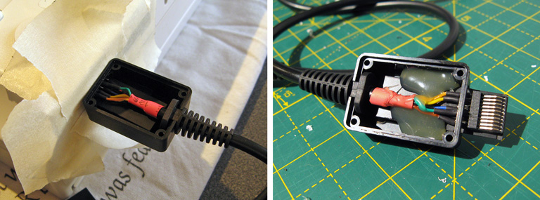
When you're completely happy with the connector, you can make it more robust by putting it inside an enclosure. I have some very small project boxes that are perfect for this sort of thing, it's a bit bulky when compared to the official Sega product but it does its job well here and doesn't bump into the power connector or AV port connector.
I cut a slot in one end of the box for the connector to stick out of and a notch in the other for the cable strain relief to clip into. I surrounded the console's serial port with a few of layers of masking tape to ensure that when the connector was inserted there was still a small gap between the case and the plug to make sure that it could always be fully inserted and not held back by interference from the case (it also protected the console shell from accidental strings of hot glue!) I then plugged the connector into the Dreamcast, made sure that everthing was neatly lined up, and secured the parts in place with copious amounts of hot glue. Once this had set I added more hot glue to the rear of the connector to make sure it was all held as securely as possible, and then screwed the enclosure shut.
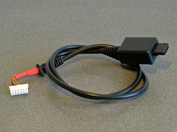
With all the effort spent on the Dreamcast end of the cable, don't forget about the MIDI interface box end! I'm fond of JST-XH connectors so crimped one onto the end of the cable, ready to plug into the circuit board. The finished cable is seen above!
Building a prototype MIDI interface cable
With a Dreamcast serial port cable to hand I was able to experiment and see what happened when using the O・to・i・re (お・と・い・れ) sequencer. Here's the circuit I ended up building on a breadboard:
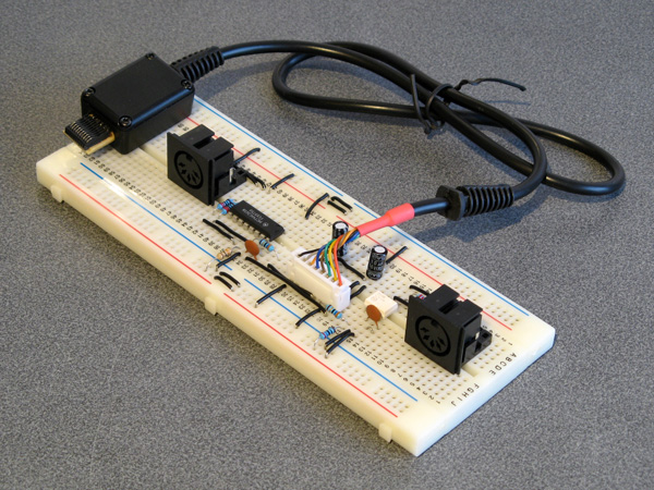
On the very left is the first serial cable connector I tried constructing. It looks more yellow than the final version as I used a piece of pad board for the backing piece instead of the 2mm ABS plastic – I thought I was going to solder the PCI Express connector piece to a circuit board rather than directly to the cable's wires, this turned out to be a mistake. One advantage is that it does have eight wires soldered to it – I thought I'd see what RTS and CTS were doing, but I ended up not using them. The MIDI port to the left is for MIDI OUT and has a large black chip to act as a buffer, the port to the right is for MIDI IN and has a small white chip as an optoisolator. Here's the corresponding circuit diagram:
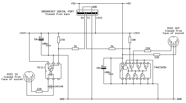
The position of the ports is flipped in this diagram when compared to photo of the breadboard, but it otherwise matches up!
On the left is the MIDI IN port. This uses an H11L1 optoisolator as they are still reasonably easy to get hold of today, are fast enough for use with MIDI and can be run directly from +3.3V. Its output on pin 4 is open collector so it needs the 270Ω pull-up resistor to the +3.3V rail. A +5V-demanding optoisolator could also have been used if it had an open collector output and the pull-up resistor on its output was still tied to +3.3V (we don't want to run +5V into the Dreamcast's +3.3V logic!) but this makes the wiring a little more complicated so sticking to a +3.3V-compatible part makes life easier.
The 36Ω resistor between the output of the MIDI IN circuit and the serial port's RX pin is there because it is in the official cable. The official cable also places ferrite beads on every I/O pin (and has a ferrite bead clipped onto the cable itself) which I have not replicated in my own cable, but they can't hurt and I suppose it could protect the console from certain direct shorts!
The MIDI OUT port uses a 74HC365N to convert from the serial port's +3.3V logic to +5V to drive the MIDI output. MIDI signals can be run from +3.3V (it's the flow of current that's more important than the selected voltage) but +5V seems more typical so I thought I'd stick with that, and as we need to buffer the signal anyway (I'm not sure how much current the Dreamcast's serial ports are designed to sink or source) using the +5V supply we have available to us made sense. The voltage threshold for a "high" input signal is probably a bit too high with the 74HC365N – +3.3V is pretty close to the recommended values in the datasheet, so the 74HCT365N version of the chip would give you more margin for error and would be a drop-in replacement. In my testing the 74HC365N does work well, though, and it's what I had available.
The cable used in this prototype has eight connections rather than the six in the final. This is because I did experiment with the RTS (pin 6) and CTS (pin 7) signals from the console, however as far as I can see these are just pulled low and high respectively and do not change from the moment the console boots, even when sending and receiving MIDI data within the O・to・i・re (お・と・い・れ) software. If they were planned to be used for some purpose then I'm not sure what, and with only one piece of software released to test with I'm not sure I'll find out.
In any case, with this circuit data from the MIDI IN port is translated to +3.3V logic levels suitable for the Dreamcast's serial port input (RX) and translated back from the serial port output (TX) to a current loop suitable to drive a device connected to the MIDI OUT port. In practice it seems this MIDI OUT port acts more like a MIDI THRU with the O・to・i・re (お・と・い・れ) sequencer – any data sent to the MIDI IN port comes straight back out of the MIDI OUT port, however if you record some notes in the sequencer and play them back afterwards they aren't played back out of MIDI OUT. At first I wondered if I'd made a wiring error (accidentally connecting MIDI IN straight to MIDI OUT) but the MIDI OUT is indeed under control of the software as it will stop relaying messages on certain screens.
Putting it all together in a nice box
I ended up using my usual pad board construction technique to build the final device:
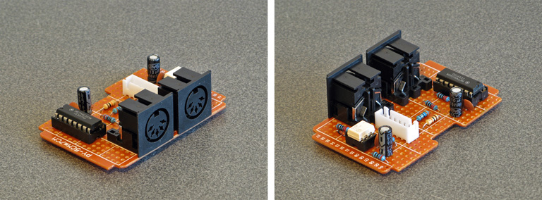
I followed the circuit diagram I'd drawn earlier (rather than copy the breadboard circuit) to ensure the diagram was correct. This was all assembled to fit in a ready-made ABS enclosure, into which I cut some holes. Historically I've had a hard time cutting neat round holes in plastic enclosures – I have a few hole saws and these are great for cutting through wood or acrylic but when trying to cut ABS they tend to bind and either rip the box out of the vice or just shatter it. I normally resort to drilling lots of very small holes around the perimeter of the circle and then try to file it to size, which is OK for buttons or sockets with overhanging parts to hide the inaccuracies but wouldn't do here! For this project I bought a very cheap step drill set on eBay (three bits for a fiver) with zero expectations but it did an excellent job, it kept the centre hole I'd started from and didn't need very much cleaning up. I wish I'd bought one sooner!
The other enclosure challenge to deal with was labelling the two ports. I normally get away without labelling my projects because the function of each port can be guessed quite easily (e.g. inputs and outputs normally only plug in one way, or player 1 is on the left and player 2 is on the right) but in this case there's not much convention for where MIDI OUT and MIDI IN go (though the original Dreamcast MIDI interface cable puts MIDI OUT on the left, as does my M-Audio Midisport). For this I thought I'd try using some dry transfer lettering designed for model-making, and it seems to do a great job!
I'm pretty happy with the final outcome – it's a bit of a pain making the serial cable for connection to the Dreamcast, but the end result works well and it saves spending an absolute fortune on the original Sega accessory.
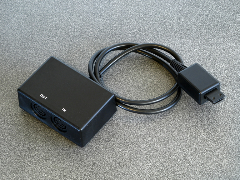
Now I can get on with making music with my Dreamcast!
The completed Light Phaser to Justifier adaptor
Wednesday, 29th April 2020
Since my previous post I've had a chance to test the Sega Light Phaser to Konami Justifier adaptor circuit with Lethal Enforcers II: Gun Fighters and it seems to work well throughout the game so I thought it was a good time to put the project into a neat box.
The Mega Drive uses common DE-9 connectors for its controller ports. You can easily find metal connectors with lugs for panel mounting however I wanted to use plastic connectors similar to the ones on the original console – not just for a consistent look, but to also protect the plastic connectors on the Sega Light Phasers from being scratched by the sharp edges of metal connectors. I'm using controller extension cables for the nice moulded connector and cable that plugs into the console, so thought I'd look at the controller socket end. Squeezing the bottom half of the connector splits the two halves apart and you can use a spudger or similar tool to pop the casing open and retrieve the connector – just what I needed!
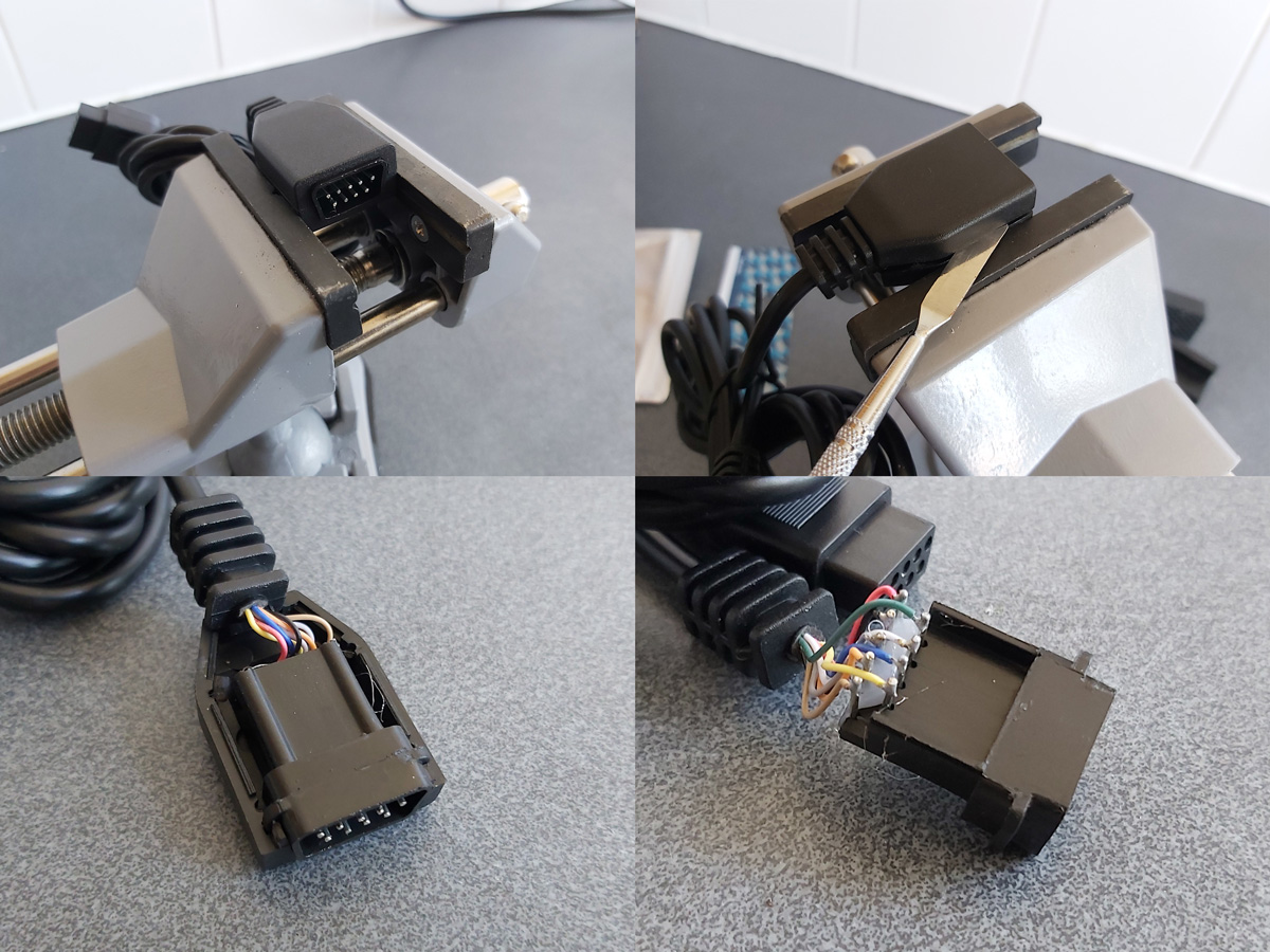
I nearly always put my projects in off-the-shelf enclosures, cutting and drilling holes in them where required. In this project's case the most awkward holes to cut will be for the controller connectors as they do not have an external lip to mask any poorly-cut holes. As such, I thought I'd start here:
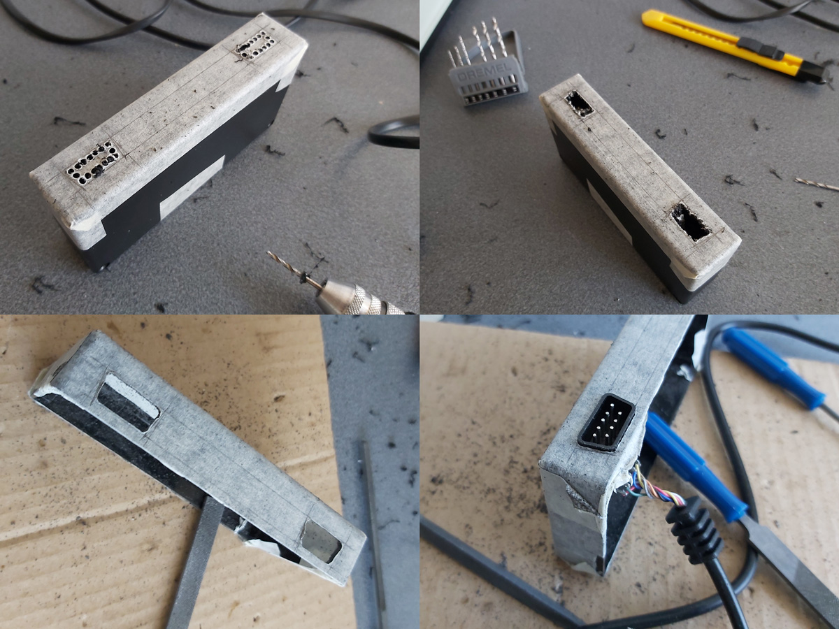
My process here is a bit tedious, but gets the job done – I cover the enclosure in masking tape, then mark out where the holes should appear. I use a drill to make several holes inside the shape I wish to cut out, then use a router bit or sharp knife to cut between the holes to open up the hole properly. A set of hand files is then used to bring the hole to its final shape and size, checking against the connector along the way to ensure an accurate fit.
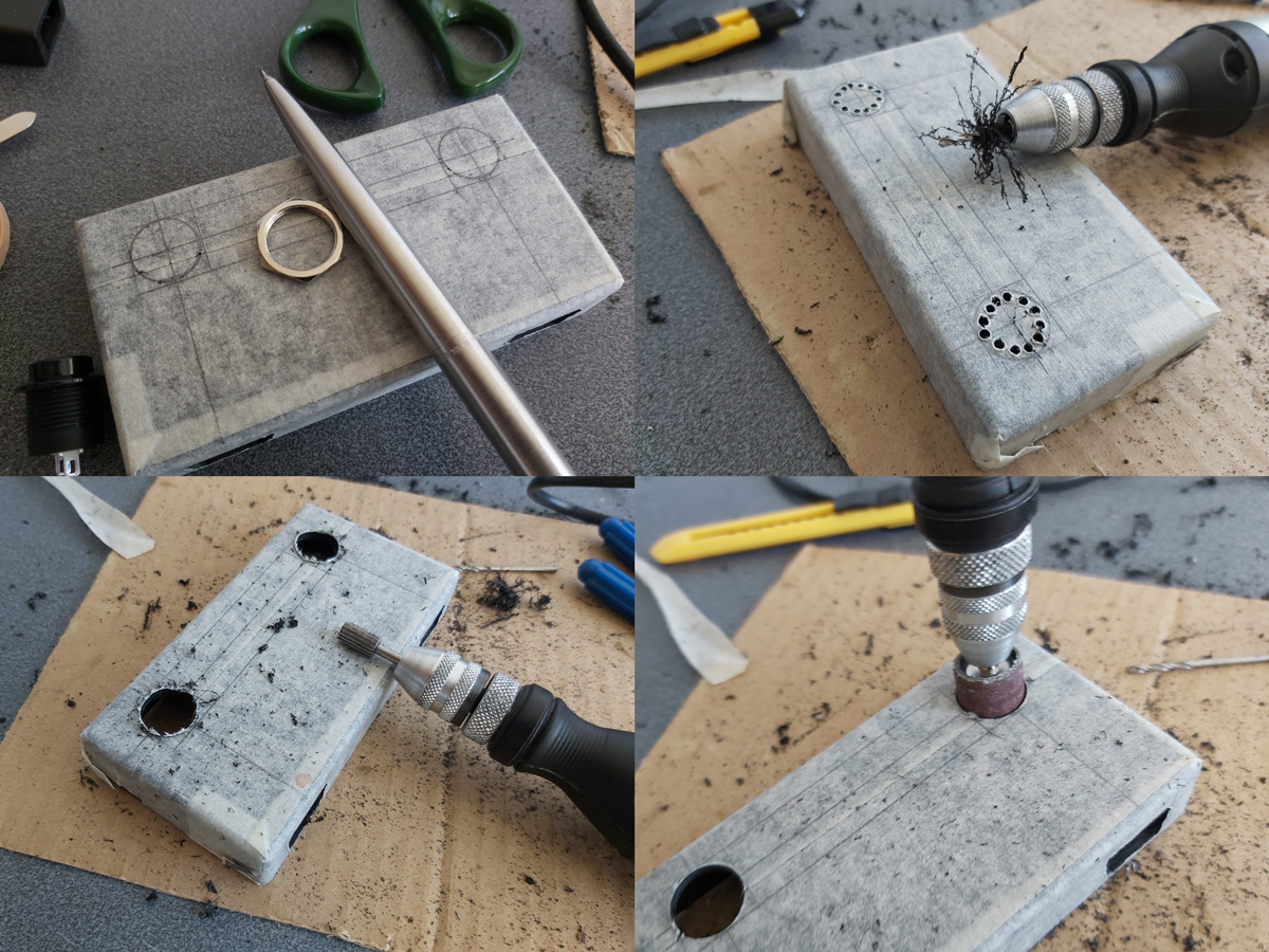
The circular holes for the buttons are cut in a similar fashion, except that as the buttons have outer lips that cover the borders of the hole the outer edges don't need to be quite as precise and a larger router bit and drum sander can speed up the job considerably rather than having to rely on careful hand filing.

A rectangular notch was cut in the rear centre of the case for the cable to the console to exit through and the parts were then loosely installed for a test fit. A piece of pad board was cut to size by scoring it and snapping it over the edge of a table. I wanted it to be as large as possible to make it easier to fit all of the components and wires in, but could the case be closed with the cables and connectors in place too? To make sure it would I thought I'd start with the bulkiest of cables, the one that goes to the console.

I attached a nine-pin crimp connector to the end of the controller cable to plug into the pad board and experimented with the placement of the destination connector – I found that four rows down was about the closest it could go to the top edge of the board whilst still providing enough room for the cable coming in to bend neatly out of the way.
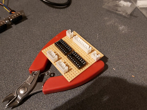
The various parts for the console output connector, light gun input connectors, start button connectors and multiplexer chip DIL sockets were placed on the pad board without soldering to get a rough idea of the final layout and component spacing, ensuring there was enough space around each part to install other components or wires. Once a rough idea was in mind, the main soldering work could begin!
Not much appears to happen between the first and final stages, as most of the work takes place in the wiring on the bottom of the board. Connections that can be made in straight lines without crossing other connections are soldered first, followed by straight connections that cross other connections that can be insulated by slipping on a piece of insulation stripped from a reel of wire. When all of the easy connections are made in this way the outstanding connections are made by soldering lengths of thin wire wrap wire between points on the underside of the board. As each connection is made it is crossed off the circuit diagram – this allows me to check that the circuit diagram is correct, as if I can replicate the circuit from this diagram it's a pretty good indication that it's safe for other people to use to make their own versions of this project.
The DE-9 sockets used for the Light Phaser inputs have all nine pins soldered to the cable by default. We only care about four of them (VCC, GND, TL and TH) and as we don't have enough room for all nine connections to be soldered to the board four-pin connectors are used instead. The old wires are unsoldered and new wires and crimp connectors are attached in their place. This let me check that the circuit board was otherwise working fine, but I still need to figure out how to mount these connectors securely inside the enclosure. I was initially thinking of just holding them in place with hot glue, but this is not very elegant and makes future maintenance much harder! The DE-9 sockets do have a flat surface at the top that is only slightly more than 5mm from the top surface of the enclosure, and I do have some 5mm PCB standoffs that could be handy…
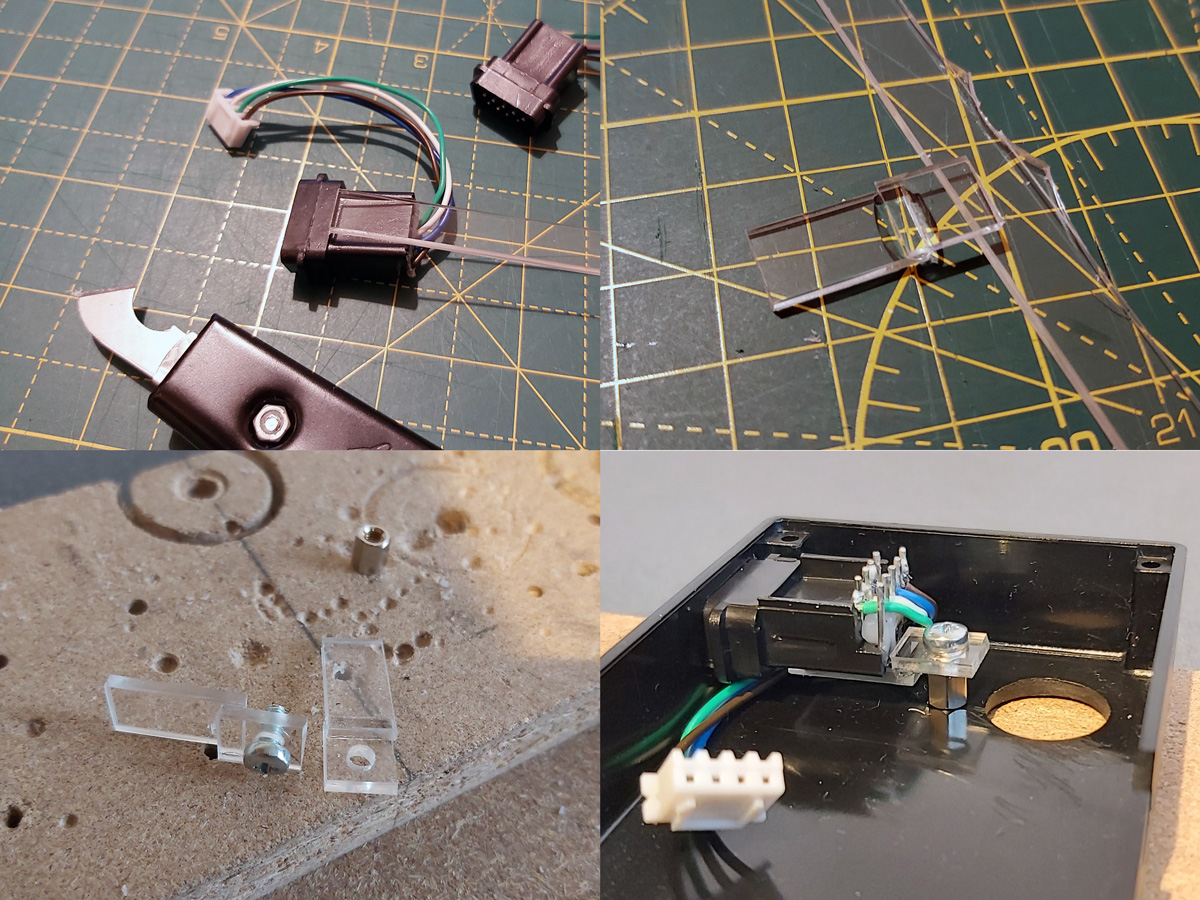
I cut a 9mm wide strip of acrylic from 2mm thick sheet which fits neatly into the top channel of the DE-9 connectors. I then cut it into short sections that could be glued together into Z-shaped brackets. The long section of the "Z" mounts to the DE-9 connector and the short section has a hole drilled through it so it can be secured to the PCB stand-off with a screw. The arrangement is then test fit inside the enclosure using double-sided sticky tape to check that a solid mount is possible – the screw to the PCB stand-off accounts for one part of that mount, and the tight fit of the connector inside the D-shaped hole in the enslosure accounts for the other part.
When it seems like a good fit is possible the Z-shaped brackets are glued to their DE-9 connectors. The DE-9 connectors are then installed in the enclosure with some glue on the bottom of the PCB stand-offs – when everything is lined up neatly this glue secures the stand-offs in the right position, albeit not very strongly.
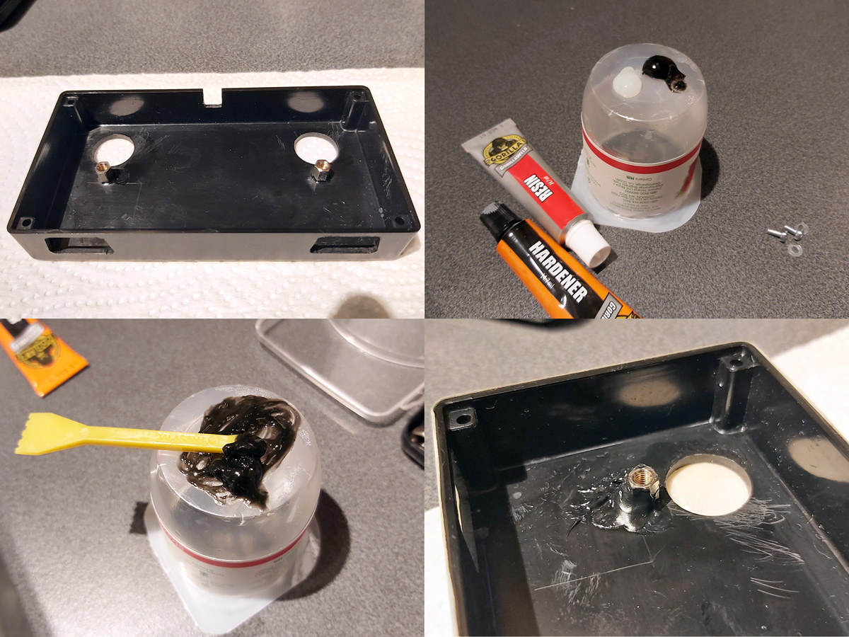
Once the glue had set the screws were removed and the DE-9 sockets were carefully removed. Two-part epoxy was then applied liberally around the PCB stand-offs to provide a bit of extra support. Unfortunately, the stand-offs are very close to the nuts used to secure the start buttons to the enclosure and as such not much epoxy could be placed on that side but hopefully the rest should provide enough support.

Whilst the epoxy was curing the final parts of the project could be assembled – a pair of start buttons had wires soldered to them with crimp connectors on the other end and a couple of rubber strips were cut to provide a bit of extra grip to the bottom of the adaptor. The various component parts of the project can be seen in the photo above.
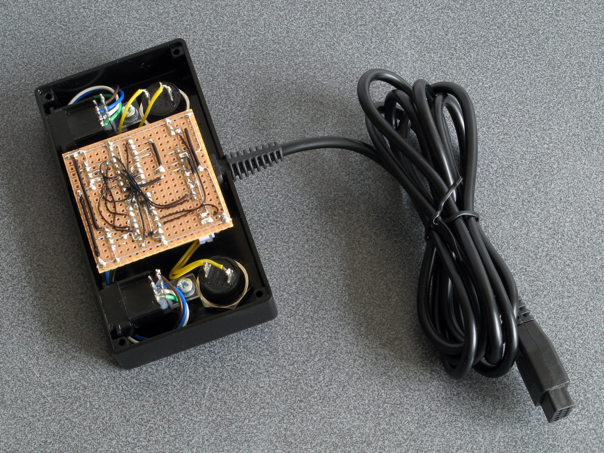
Everything does fit fairly neatly inside the enclosure, fortunately! After everything is assembled inside the bottom of the enclosure was screwed on and the rubber grip strips attached with double-sided sticky tape.
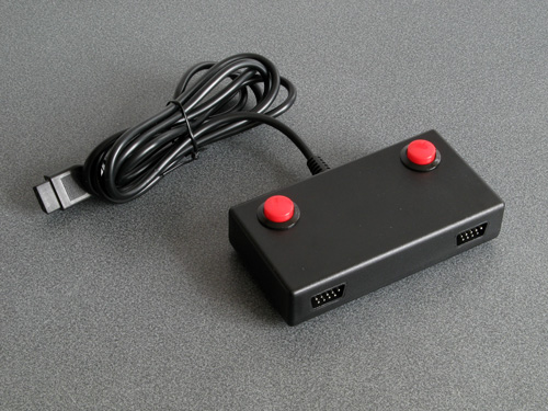
I still haven't been able to test this adaptor with any Mega CD games however it does work well in both Lethal Enforcers and Lethal Enforcers II: Gun Fighters on the stock Mega Drive so hopefully it will also work well in Mega CD games.
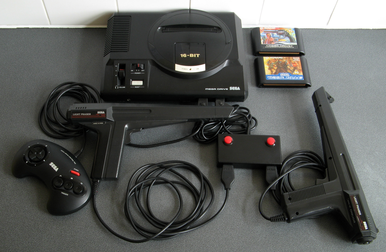
I'm pretty happy with how this project turned out. If you would like to assemble the adaptor yourself, you can find the schematic in the previous journal entry, and if you do build it I'd love to hear how you got on!
Adding some protective resistors to the Light Phaser to Mega Drive gun adaptors
Monday, 20th April 2020
Here's a quick update to the two Mega Drive light gun adaptor circuits, all to a few extra resistors in and around the adaptor and the console.
The real Sega Menacer receiver drives the TH line (used to indicate when the gun has seen light) directly from the output of a NOR gate with a 470Ω resistor in series. My circuit uses a transistor in the open-collector configuration with a 10KΩ resistor on the base input and a 1KΩ pull-up resistor, which is the same as the circuit used in the original Sega Light Phaser.
In a worst-case scenario the console could configure TH as an output, drive it high, and the Menacer adaptor could drive TH low at the same time. This would short the console's TH output to ground via the transistor, and might damage it (I'm not sure how these I/O ports are constructed internally). The TH output from a regular Sega Light Phaser would have the same problem, however that only pulses low briefly when it sees the light from the CRT whereas the TH output from the Menacer adaptor is latched and can stay low for a much longer time, increasing the risk. Resistors are cheap, so assuming the engineers at Sega know their hardware better than I do I thought it safer to add a 470Ω resistor on the TH output. This hasn't affected performance, as far as I can see. I also corrected the diagram to reference the BC548 as this is the transistor I tested with – the BC547 probably works too, however in the interest of accuracy I thought it best to stick with what I know works.
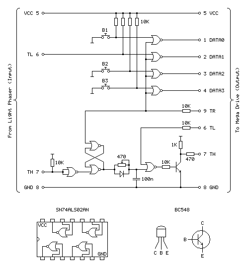
Sega Light Phaser to Sega Menacer adaptor
The Menacer circuit (as well as the original control pad) drives the DATA0~DATA3 lines directly so I haven't included any resistors there. I have, however, applied the same resistor changes to the Justifier adaptor:
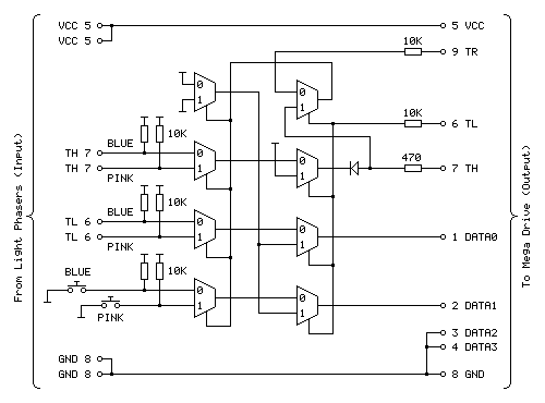
Sega Light Phaser to Konami Justifier adaptor
As well as the 470Ω resistor on the TH input/output line I have added the 10KΩ resistors on the TL and TR input lines. I'm still not sure what these are for but as they are there in the Menacer adaptor and as Sega presumably know best I've included them here for completeness. As these are attached to inputs on the logic gates there should be very high impedance anyway, but it could be for protection in case the logic gates are improperly powered. What I do know is that the extra 10KΩ pull-ups on the TH inputs from the Light Phasers should protect against spurious TH outputs when either of the guns are unplugged.
I still haven't been able to test the circuit with any other games, but for now these two circuits seem to be holding up!
Simplifying the Light Phaser to Justifier adaptor to a two-chip solution
Saturday, 18th April 2020
In the previous post I mentioned I was dissatisfied with the optimisation of the Light Phaser to Justifier adaptor circuit. This was because I was using two quad two-input multiplexer chips (eight multiplexers total) but only using three multiplexers on each chip but also needed two inverter gates and so had to add a third chip to accommodate that requirement. It seemed like there must be a better solution, and after pondering this in the shower I think I found it.
One of the inverters is required for the transistor used to drive the TH line from the circuit. The TH line is bidirectional, and from our end of the circuit is either left floating (where it can rise high) or pulled directly to ground. To achieve this I was using an NPN transistor with the collector connected to TH, the emitter connected to ground and the base connected (via a resistor) to our logic signal. Unfortunately, such a transistor is switched on by a positive voltage and so a logic high at the input resulted in a logic low on TH, so to correct this an inverter was added.
A much simpler solution is to get rid of the inverter and transistor entirely and to replace it with a reverse-biased diode, replacing three components with one:
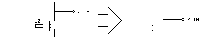
Current can only flow the diode if the voltage at the anode (right, connected to TH) is higher than the voltage at the cathode (left, connected to our logic signal). This means that if our logic signal is the same as the current state as TH then no current flows (and so we leave TH alone) and if our logic signal is high and TH is low then the diode is "backwards" and no current flows. The only way we can influence TH is if it is high and our logic signal is low, allowing current to flow through the diode, grounding TH – which is our desired outcome. One inverter is out of the way!
The other inverter is used to produce an inverted version of TH which is used when the console is retrieving the peripheral ID from the Justifier. We can use a multiplexer as an inverter by using the select pin as the input, tying the "0" input high and the "1" input low (that way when 0 is requested 1 is output and when 1 is requested 0 is output). The problem we have here is that all four multiplexers on a chip share a common selection pin, we need to invert TH, and neither of our two multiplexers is using TH as the select pin (one is using TR to select between the two guns and the other is using TL to globally enable or disable the guns).
The solution here is that we only need this inverted TH signal during the peripheral ID check which is carried out when the guns are globally disabled. When the guns are disabled we don't care about what the TR gun-selection multiplexer is doing, as whether the blue gun or pink gun is selected is irrelevant as the data never makes it to the console. We can therefore use the spare multiplexer on the TL-selected multiplexer chip to select between TR and TH, and use the output of this as the select pin into the multiplexer chip previously used to select between the two guns and use its spare multiplexer as the inverter.
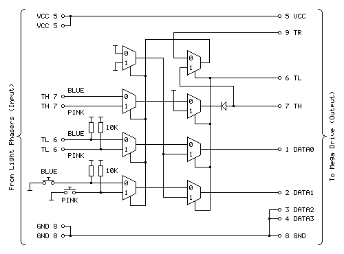
The revised circuit is shown above, the wiring is more complicated than the previous one however it takes advantage of all eight multiplexers on both chips and does away with the need to have an additional inverter logic chip and transistor driver circuit for TH.
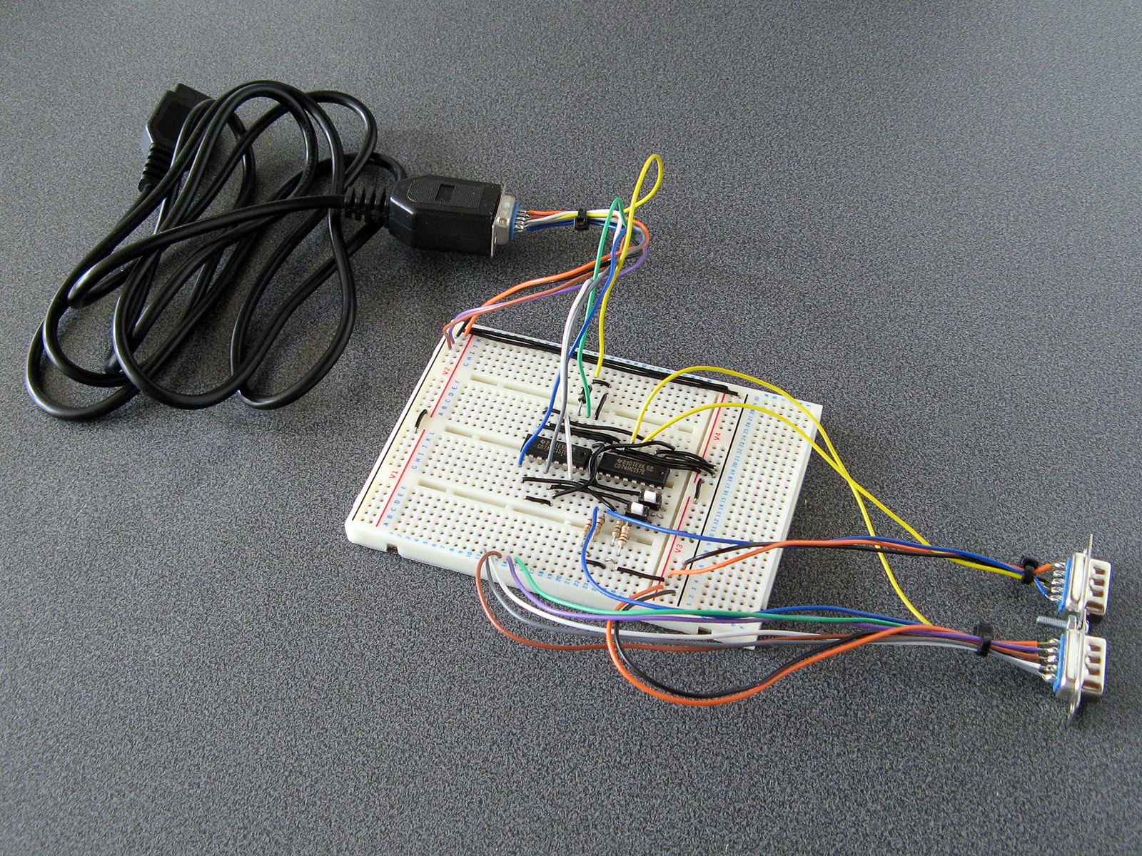
The revised two-chip prototype is picture above, and has been tested successfully with Lethal Enforcers – performance doesn't seem to be any different from before, which seems to be a good sign!
Using Master System Light Phasers to play Konami Justifier games on the Mega Drive
Saturday, 18th April 2020
Following my adventures with building an adaptor that lets me use Sega Light Phaser guns in Sega Menacer games it seemed sensible to turn my attention to the other type of light gun for the Sega Mega Drive – the Konami Justifier.

These guns are unsurprisingly incompatible with the Sega Menacer and Sega Light Phaser and supported in even fewer games on the stock Mega Drive (only Lethal Enforcers and Lethal Enforcers II: Gun Fighters). However, these games are more in line with the type of light gun game that I like to play than what you'd find in the Menacer's library (even though the digitised sprites haven't aged particularly gracefully) and the guns are eye-wateringly expensive if you want to get a set of both for two-player games which makes the idea of a cheap adaptor to use the Master System's Light Phaser more appealing. And, of course, it's a fun challenge!
You may have noticed that the two guns in the photo at the top of the post are different colours, and unfortunately this is not purely cosmetic. The Justifier comes in distinct "player 1" and "player 2" variants, with the first gun plugging into the console and the second gun plugging into the bottom of the first gun using a modular connector in a daisy-chain configuration. This allowed Komani to sell console-specific blue player 1 guns and a generic pink player 2 gun that would work with the blue player 1 gun from any system. If you invited a friend over to play with you then you'd need to go out of your way to buy the specific player 2 gun (your friend's blue player 1 gun won't work), and as the blue gun was not sold separately you couldn't buy a game and "upgrade" to a light gun controller later, you'd need to buy one that came with a game and as a result both guns are now somewhat difficult to find and fairly expensive, especially the player 2 gun.
However, this arrangement should allow for a pretty neat solution where we can build a single adaptor that plugs into a controller port on the Mega Drive and provides two controller ports for the two Light Phaser guns rather than having to build two separator adaptors. Like the Menacer, the Justifier does have an extra button when compared to the Light Phaser however it's only one button this time (rather than three) and it's used as a Start button so both of these could be put on the adaptor unit itself between the two players.

A Point Blank arcade machine with two Start buttons on the control panel between the two guns.
Without buying a pair of Justifier guns, how can it be studied so an adaptor can be built? In the case of the Menacer the receiver units can be bought cheaply and studied to figure out how they interface with the console and the patent document covers how it should work in high-level detail too. I have been unable to find such information for the Justifier. Fortunately Eke-Eke, the author of the Genesis Plus GX emulator, came to the rescue with the document gen_lightgun.pdf which goes into some detail about how the Justifier interfaces with the Mega Drive.
The key information to take into account here is that DATA0 is mapped to the trigger, DATA1 is mapped to the start button, TH is used for the light sensor, TR is used to select which of the two guns to query and TL is used as a general gun enable/disable line. As both guns share the same data lines for their triggers, start buttons and light sensors we can use multiplexers to select between the two guns.
The Mega Drive also needs to be able to detect when the Justifier is plugged in, and it does this by checking the state of the four DATA lines, once when TH is high and once when TH is low, then combining the bit values read in both states to form a single four-bit peripheral ID. The process was explained in more detail in an earlier post, however for the sake of simplicity to correctly return the device ID of %0001 we need to make sure that when TH is high all four data lines are low and when TH is low DATA2 and DATA3 should still be low and one or both of DATA0 and DATA1 should be high.
As DATA2 and DATA3 are always low and aren't used anywhere else they can just be tied low at all times and that should work. DATA0 and DATA1 should pass through the trigger/start button status (active low signals, so normally high) when the game is reading the button state but it looks like they should be forced low when TH is high. According to Eke-Eke's documentation: "I'm not sure why Justifier returns such values, maybe setting TH=1 will force input lines to 0".
My first attempt, therefore, was to use a NOR gate outputting to each of the two data lines with one input to each coming from the TH line and the other input coming from the inverted trigger/start button status. This way if TH was high both data lines would be forced low, otherwise it would output the inverted form of the input (and as the input to the NOR gate was already inverted, the final signal would be corrected – two wrongs do make a right in electronics!) This would not work if both trigger and start button were pressed, unfortunately, but maybe that wouldn't be a problem?
Happily, this worked in the menu for Lethal Enforcers, with the adaptor plugged in I was able to select the option to start a one- or two-player gun game! However, the game was completely unresponsive to the buttons. When writing an emulator you can make certain assumptions about how the hardware works, as long as the right values are in the right places when the software reads them. You also have the advantage of being privy to the internal state of the hardware that external devices might not be able to see! One important note in Eke-Eke's documentation is "this means the Justifier should return the following byte values when TH is set as output" – we can't directly tell whether a pin is set to an output or an input from outside the console, we can only see what its current signal level is. During normal gameplay TH is an active-low signal from the light gun's light sensor, and as a result TH is normally high which blocks the buttons from working. I had thought that maybe the game software would drive the TH pin low during its button-reading routine to allow the data to pass through but evidently the gun doesn't work this way.
Another issue is that whilst I can use a logic analyser to see what state the pins are in over a period of time, I can't tell at what point the console is reading those pins itself and making decisions based on what it sees. I could disassemble the game code to try to see how that's working, but I couldn't figure out any meaningful output from the disassembly tools I tried and couldn't find an appropriate debugging emulator so went back to trial and error.
The solution, I think, is in the TL pin being used to enable or disable the guns. I think that we should only mess around with forcing DATA0 and DATA1 high or low (based on the state of TH) when the guns are disabled, otherwise we let the button and light sensor state pass through. We can achieve this with two stages of multiplexers, one to select between the two guns (selected by TR) and another to globally enable/disable the guns (selected by TL). If we invert TH we can use this to drive the DATA0 and DATA1 lines when the guns are disabled, meaning that we also fix the problem where the gun wouldn't be detected if both buttons were held.
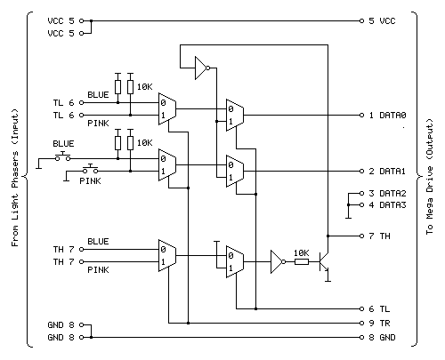
The above diagram shows the circuit I'm currently using to test with and it appears to work fairly well with Lethal Enforcers, being detected as a valid gun during startup and working in-game with both guns seemingly being handled correctly.
The first column of three multiplexers selects between the blue (player 1) and pink (player 2) gun inputs via the TR input. The top multiplexer handles the trigger (TL), the middle multiplexer handles the two Start buttons and the bottom multiplexer handles the light sensor inputs (TH). The second column of three multiplexers selects between the guns being enabled and guns being disabled via the TL input. When the guns are disabled (TL is high) DATA0 and DATA1 are driven by the inverse of TH to help provide the valid %0001 peripheral ID, allowing the adaptor to be detected as a Justifier.
The TH pin is a bit more challenging as it needs to be both an input and an output. At the moment when the guns are disabled it is driven high by tying the other input to the multiplexer high. The TH output is driven by a transistor; when the transistor is switched on it connects TH to ground (making it low) and when it is switched off it is left to float (normally floating high, but otherwise under the control of the console). As the transistor is switched on by a positive voltage this effectively acts as an inverter, hence the signal from the multiplexer to the transistor also needs to be inverted.
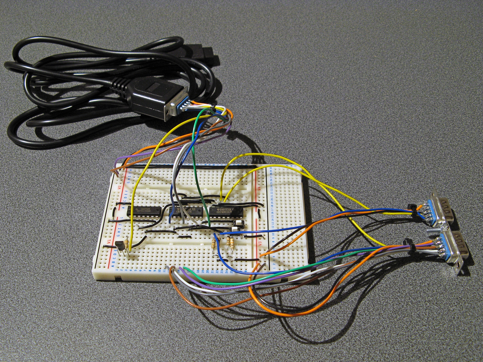
The prototype adaptor assembled on a solderless breadboard.
I'm not entirely happy with the way the circuit has been implemented, in particular the use of two multiplexer chips where only three of the four multiplexers are used and the need for an additional chip for the inverter gates. Multiplexer chips normally have a global enable/disable pin in addition to their data selector, which makes me wonder if such a pin could be useful. The 74HCT157 chips I'm using drive the outputs low when disabled which would not be very useful in this particular use case, however other chips are available that make the outputs high-impedence when disabled which may be more useful and allow for a circuit design that uses fewer parts.
There is also a slight issue of reliability and accuracy. When playing the game shots are generally fairly accurate and always register however they sometimes are offset horizontally. Eke-Eke's document points out that Lethal Enforcers does not use the console's horizontal counter latch so the inaccuracy may be a software issue – interestingly it seems Lethal Enforcers II does use the horizontal counter latch so when I can test with this cartridge it will be interesting to see whether accuracy is affected. More weirdly, the game does provide a "gun adjust" menu option where you can calibrate the game to compensate for any horizontal or vertical offset in the gun hardware however this does not seem to detect all shots and sometimes the accuracy is miles out! This also seems to be affected quite heavily by proximity to the screen, normally bringing the gun closer to the screen yields more accurate results however here it seems to make things worse. I'm not sure why this is and will continue to test the circuit to see if performance can be improved.
The completed Light Phaser to Menacer adaptor
Friday, 10th April 2020
In the last post I was having difficulty with the overall logic for handling the light sensor signal from the Sega Light Phaser and passing that along to the Mega Drive as if it was coming from the Menacer receiver. This involves latching the signal (instead of passing it along directly) and allowing the console to reset it once handled via the TR line. The signal needs to be delayed as well to simulate the delay from the overhead of the Menacer's wireless communications; without this delay the aiming is offset to the left. The signal is also gated using the TL line; I'm not entirely sure why this is done (some form of external interrupt inhibition?) but it's part of the original receiver so I thought it best to implement this for the sake of compatibility.
My main problem was that the CMOS NOR chip I had to hand was not triggering reliably with the signal from the light gun and the RC circuit used to delay that signal; I'd swapped it for a TTL NAND chip which then did work however the logic inputs to the latch were inverted (a simple NOR latch has active-high inputs and a simple NAND latch has active-low inputs) and to fix this would have required a lot of additional logic gates. I ordered an SN74ALS02AN TTL NOR chip and found that this worked very well, so have settled on the following circuit:
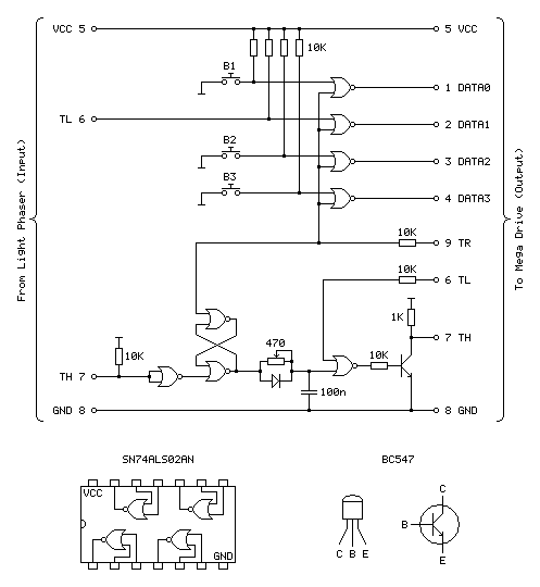
Update (20/04/2020): Please see this post for an updated diagram with a protective 470Ω resistor on the TH output
The four NOR gates towards the top of the circuit diagram are used to gate and invert the inputs from the four input buttons (one main trigger on the Light Phaser and three secondary function buttons on the adaptor itself). This is unchanged from the previous circuit and still works well.
The most important aspect of the circuit at the bottom of the diagram between the two TH pins is the latch made of two crossed-over NOR gates with the output from one going to the input of the other and vice-versa. The two inputs to this latch are normally low (TR from the console is driven directly and normally low, TH from the Light Phaser is normally high but inverted by a NOR gate with its legs tied together). When the reset pin TR goes high the output of the top gate must go low, as a NOR gate will always output low if either (or both) of its inputs are high:
| Inputs | Output | |
|---|---|---|
| A | B | Q = A+B |
| 0 | 0 | 1 |
| 0 | 1 | 0 |
| 1 | 0 | 0 |
| 1 | 1 | 0 |
If we assume that the other input to the lower NOR gate is also in its default low state then the two low inputs will result in a high output. This high input travels back to the top NOR gate's other input. This means that even when the TR pin goes back low again there is still a high input on that top NOR gate and so it maintains its low output.
When the Light Phaser sees light its TH output goes low, the NOR gate with its legs tied together inverts this to go high and the bottom input to the lower NOR gate in the latch goes high. This makes its output go low, which travels to the top NOR gate, making both inputs low (assuming TR is still low) and making the top NOR gate output a high which comes back down to the lower NOR gate so that even when the Light Phaser stops seeing light and the other input to the bottom NOR goes back to low there is still a high on the other pin, keeping the overall output low.
Effectively, what this means is that when the Light Phaser sees light the output of the latch goes low, and to return this back to a high the console needs to pulse the TR pin high.
The output of the latch goes to a delay circuit consisting of a resistor, capacitor and diode. This delay is required because the real Menacer introduces a delay between when it sees light and when it triggers the console's TH pin, and games are programmed to compensate for this. Without replicating this delay the aim is offset considerably to the left.
The logic gates are digital devices however still adhere to analogue rules and will treat certain voltages as high or low digital signals when they pass a certain threshold. The delay is implemented by slowing the rise or fall of the logic signal by charging a capacitor via a resistor, so whilst the logic signal at the output of the latch changes very quickly it will take the capacitor a while to charge or discharge via that resistor to a voltage level that is interpreted as a change of state by the following logic gate. The diode is there because we want the signal to be delayed when the gun sees light (when the logic level goes from high to low) but want it to change quickly when the latch is reset (going from low back to high again). When going from low to high there is a higher voltage to the left of the diode than there is across the capacitor to its right and so current can flow quickly through the diode, bypassing the slow resistor and charging up the capacitor quickly. When going from high to low the current can't flow backwards through the diode and so the capacitor has to discharge slowly through the resistor, providing the desired delay.
After this delay comes another NOR gate with its other input coming from the console's TL pin. I'm not entirely sure what this is for, as mentioned above, but it does at least allow us to buffer the signal from the RC delay circuit. The real receiver circuit then uses a final NOR gate with its inputs tied together to invert the latched signal before passing it to the console via a 470Ω resistor, but as I am already using an extra NOR gate to invert the input from the Light Phaser and have therefore used all four gates on one chip I instead use a transistor with a 1K pullup to invert the signal. The Light Phaser uses such a transistor circuit with the same 1K pullup resistor on its TH output so I thought it safe to use it here as it would be electrically compatible. The real receiver also includes 10K series resistors on its inputs from the TR and TL lines – I'm not entirely sure why but in case there was a good reason I thought I should use them here also!
With the circuit appearing to work well I thought it was time to put it in an enclosure. I found a box that was a comfortable size to hold in one hand – it's about the same overall size of a Master System control pad other than being quite a bit fatter. This allowed me to put the three push buttons down the side of the box so they can all be pressed easily when gripping the box in one hand. The lid of the box has a lip that would interefere with the ability to tighten the nuts for the buttons and so I cut a small piece of acrylic that is slightly thicker than the lip and short enough that the box can be closed with it in place.
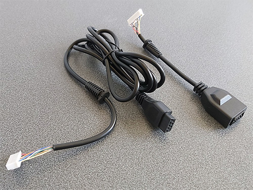
Of course, we need something to plug the Light Phaser into and a cable to plug the adaptor into the console with. A good source for these connectors is an inexpensive extension cable, so I bought one and cut it in two so I could use it for this project. After cutting the cable in two I installed strain reliefs and crimp connectors, and definitely remember to do that in that order! Interestingly I've bought a few of these cables recently from different suppliers (and with different moulding designs for the console plug and controller socket) and they've always been about half the length advertised but sold in packs of two.
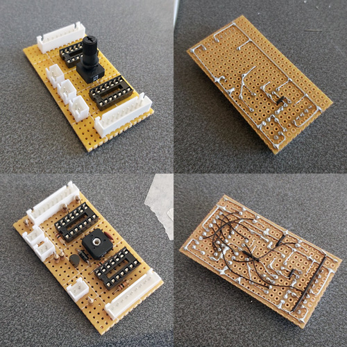
I normally use pad board to solder my final circuits together. I start by roughly placing the components on the board where I think they should end up going, and when I've got the main parts in place I flip the board over and start soldering them down, using bare pieces of wire to make connections between components. I lay the bare pieces of wire as straight as possible and try to avoid crossing them over; where necessary I'll add a piece of insulation to a wire where it needs to cross another. Once as much of the board is placed in that fashion I'll solder thin wires between the points that can't have direct connections. It may not be the prettiest job (and making corrections afterwards is a bit of a pain) but it's worked well for me and I've found it allows for more compact layouts than stripboard.
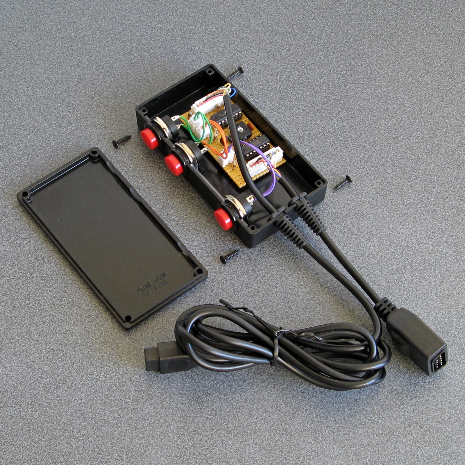
Some crimp connectors were then added to the three push buttons and the whole circuit was installed in the box. Before the lid was screwed down the delay to correct the horizontal aim was calibrated using the 470Ω variable resistor. To adjust it the variable resistor was first set to its smallest resistance value and the tip of the light gun was touched to the centre of the screen. The aiming reticle is quite far to the left by default so the resistance of the variable resistor was then gradually increased to move the aiming reticle in the game right until it sits under the tip of the gun. The aim was then checked at the extreme left and right sides of the screen and if there were any dead zones the variable resistor was adjusted to move the aiming reticle away from the edge of the screen until it had a good range of motion across the entire width of the screen.
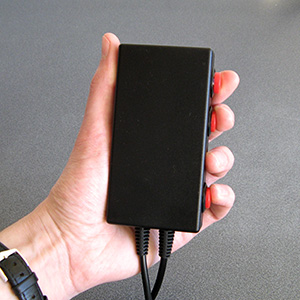
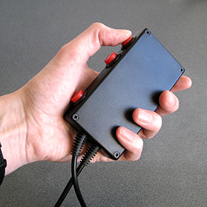
The two different grip styles for the adaptor buttons
The adaptor can be gripped in two different ways – in the regular position you have direct access to all three extra buttons with your fingers, and in the reversed position you have access to a single button at a time with your thumb. None of the games I've played on the Mega Drive use more than two extra buttons (and usually one of those is the bottom "Pause" button) but it's always good to have options!
I have tested the adaptor with the three Mega Drive games that support the Menacer — the six-in-one pack-in cartridge, T2: The Arcade Game and Body Count and am happy to report that it works with all three. I am not going to be able to test it with any Mega CD games as I do not have a Mega CD or a compatible flash cartridge, I'm afraid to say, but hopefully it will work just as well with those games.
The red and black theme was chosen to match the other accessories and I think it fits in rather well, even if it is a bit boxy-looking. If you are reading this and build the circuit yourself I'd love to hear how you get on!
Fixing the Menacer detection but breaking the accuracy of the aim tracking
Thursday, 26th March 2020
Since the last post about my experiments with using a Sega Light Phaser to play Mega Drive games I've had some good results and some disappointing ones that I'm still trying to work through.
The easy problem to solve was the handling of the buttons and making sure that the gun continued to be detected as a Menacer whenever a button was pressed. The previous circuit used active-high buttons (including an inverter to convert the active-low trigger from the Light Phaser into active-high signal) gated using the console's TH line via an AND gate. This meant that each button output a 0 when not pressed and 1 when pressed when TH was high, or a 0 in all cases whether TH was low or high.
When looking at the patent for the Menacer it became apparent that the button data lines were coming from a four-bit counter that is reset by the console's TR pin going high. When looking at logic analyser traces from T2: The Arcade Game we can see that TR is held high during device detection at the main menu screen but goes low during gameplay, being periodically pulsed high when the game alternates between handling light detection (short pulse) and reading button presses (long pulse). Rather than active-high buttons with AND gates, active-low buttons with NOR gates would seem to work better, so I ordered some NOR gate chips and tried the following circuit:
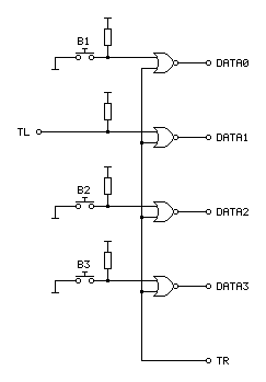
In the diagram above the TL on the left comes from the Light Phaser and the connections on the right go to the Mega Drive.
An OR gate will output a 1 if either of its inputs is a 1, to output a 0 both inputs have to be 0. A NOR gate inverts this output, so will output a 0 if either of the inputs is a 1 and will only output a 1 if both inputs are 0. When TR from the console is 1 it therefore forces the output to always be a 0, however if TR goes low to a 0 then the output is 0 if a button is released and 1 if a button is pressed – just what we needed.
Testing with T2: The Arcade Game I found that all of the buttons still worked during gameplay, and when pressing a button at the main menu the gun continued to be detected as a Menacer unlike the previous buggy implementation. All good so far!
I wanted to test with some other games, so ended up buying a copy of the six game cartridge that was originally bundled with the Menacer. I paid a little bit more and got a copy that came with the IR receiver, which is not much use without the gun however I thought it still might provider some interesting clues as to how to convert the signals from the Light Phaser to the Menacer protocol more correctly.
When the cartridge arrived I plopped it into my Mega Drive and was happy to see that the games mostly worked fine without any further tweaking. There was one fly in the ointment, however, an occasional message about the screen being too dark:
"The screen is too dark".
It would only do this occasionally when launching one of the six games and would then reset to the main intro and menu screen after shooting. Oddly, once a game was started I could quite happily move away from the TV to the other side of the room and the gun still worked reliably, so I'm not sure if this genuinely is an issue with the screen being too dark or if it's some problem with the way the gun is triggering the TH line on the console to indicate when it's seen light.
To try to get to the bottom of the issue I took apart the Menacer receiver and started sketching a circuit diagram based on the counter and NOR gate chips on the board. I then compared my scribbles to the circuit diagram in the patent, and found that the final implementation does appear to match the diagram in the patent pretty much exactly (I can't tell for certain as quite a lot of the circuitry is enclosed in a metal can, but all of the circuitry relating to the counter and NOR gate latch matches). This meant I was able to match up the console's pin connections to the diagram, which are unlabelled in the patent:
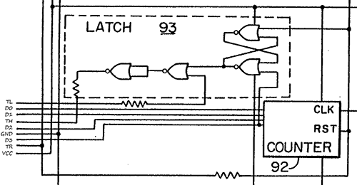
Pin connections for the Menacer receiver
It's not particularly clear due to how closely-packed the connections are in the diagram, however the important details are as follows:
- D0~D3 are connected to the counter directly, with D3 also going to set the latch at the top.
- TR resets the counter and the latch.
- TL appears to inhibit the output of the latch.
- TH only needs a 470Ω resistor between the output of the latch and the input to the console, not a common-emitter transistor driver.
I thought it would be neat if I could combine the function of the latch and the counter, so purchased a CD4017B decade counter chip as this has a handy clock inhibition input and wired it up as follows:
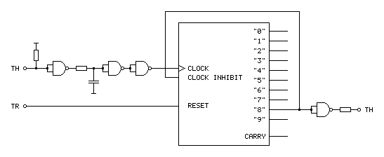
The clock input to this circuit comes from the TH output of the Light Phaser gun. This is an active-low signal so it needs to be inverted to properly clock the counter chip on the rising edge of the signal. It also needs to be delayed slightly for proper horizontal aiming (described in the previous post) so hence the additional RC circuit before the signal is fed to the counter chip.
With such a decade counter one of the 10 outputs labelled "0" to "9" is active at a time. After resetting the chip (by pulsing the reset pin high) "0" is high and "1" to "9" are low. When there is a rising edge at the clock input the chip counts up, so "0" goes low and "1" goes high, then "1" goes low and "2" goes high and so on and so forth. The "carry" output provides a rising edge clock signal when the counter overflows from "9" back to "0", allowing multiple chips to be chained together.
In the Menacer receiver the counter triggers the TH output latch on the fourth bit of a binary counter, i.e. when it reaches 8, so I've used the output of "8" as the output of the circuit. I've also fed this output back to the "clock inhibit" input of the counter chip. When this pin is low (which "8" will be when the counter is reset) it allows the counter to count up normally whenever the clock pin is pulsed. When the pin goes high (which "8" will be when we've seen eight pulses of light from the gun) it will inhibit the counter from counting any further, effectively locking it at "8". The only way out of this condition is to reset the chip, which the console does by pulsing the TR input line.
The only additional complication is that the console still expects an active low signal from the gun, so the final step is to invert the output from the counter.
Unfortunately, this does not work at all well. Games no longer seem to produce the "The screen is too dark" message, however aiming is extremely laggy and inaccurate. Checking the output of the counter with a logic probe seems to indicate erratic triggering. Using a different output from the counter (e.g. "4" or even "1") so that the counter "latches" sooner seems to improve things slightly but overall performance is still far worse in this arrangement. I'm not entirely sure why!
My next attempt was to simplify matters by using the exact latch circuit composed of NOR gates described in the patent, which worked just about as badly – the circuit still triggered eratically and accuracy was very poor. I have had issues with circuits not triggering properly before when using particular logic chips (it's why the circuit for my LCD Shutter Glasses adaptor has SN74LS14N Schmitt-trigger invertors on the logic inputs) so I thought I'd try replacing the CD4001B CMOS NOR gate chip I was using with the SN74ALS00AN TTL NAND gate chip I was using in previous experiments. The logic for a latch built from NAND gates is inverted to the logic of one built from NOR gates so it wasn't a straight swap but I don't have any other NOR gates in my parts bin. Somewhat surprisingly, with this new chip performance was greatly improved, though still not quite right.
For my next set of experiments I'm going to try replacing the CMOS NOR gate with the TTL NOR equivalent, though as that will involve waiting for parts to turn up in the post I thought I'd write a quick update on where I am so far. Fingers crossed this issue can be resolved easily and with a simple circuit!
Using a Master System Light Phaser in Mega Drive Menacer games
Wednesday, 18th March 2020
I'm a big fan of light gun games and have guns and games for most of the Sega systems – the Master System's Light Phaser, the Saturn's Virtua Gun and the Dreamcast's gun all get plenty of use.
One notable omission is the Sega Mega Drive and its Menacer light gun. This is a wireless gun with a range of bulky plastic accoutrements that represented Sega's efforts in the 16-bit generation; unfortunately only three games were released for it on the Mega Drive – a six-in-one collection of minigames that came bundled with the gun, a port of T2: The Arcade Game and the ferociously-expensive Body Count.
Ultimately the gun was a flop and they are not cheap to pick up second-hand (and are often missing most of the bits) so I haven't sought one out, however I did recently buy a cheap job lot of games which included a loose copy of T2: The Arcade Game.
I tried the game with the regular control pad and found it a disappointing experience (as most light games are when played with a pad!) so thought I'd see if I could get it to work with one of my Master System Light Phaser guns.
Of course, the game wouldn't detect that the gun was plugged in. Controllers on the Master System were generally very simple affairs, with one pin on the controller port per button (no multiplexing or serial data transfers here). On the regular control pad four data lines were used for the d-pad directions and two data lines (TL and TR) were used for the two buttons. These data lines were pulled high by the console and the control pad just contained switches that connected these data lines to ground when pressed for simple active-low logic.
The Light Phaser doesn't make use of the four d-pad data lines and only has one button so only uses one of those two data lines (TL) however it does make use of another pin on the controller (TH) for its light sensor. When this pin goes low the console latches the video chip's horizontal counter and the game software can read this and the free-running vertical counter to determine what point on the screen the console was outputting at the point the gun "saw" the light from the TV (and from this work out where the gun is aiming).
The Sega Light Phaser being used to play Rescue Mission on the Master System.
The Mega Drive is descended from the Master System's design and has very similar controller ports. The d-pad's four data lines are named DATA0 to DATA3, and by default the B and C buttons are mapped to the two TL and TR inputs like the two buttons on the Master System controller. However, the Mega Drive controller adds two extra buttons (A and Start). These two extra buttons share the TL and TR data lines and whether they are B and C or A and Start depends on the state of the TH line which is configured as an output from the console.
This use of the TH line to choose which buttons are mapped to which data lines is also used for controller identification. When TH is high the d-pad is mapped to the four data bits as normal. However, with a normal controller, when TH goes low data lines 2 and 3 (corresponding to left and right) go low also. This is normally impossible, as you can't physically press left and right simultaneously on a Master System controller, so a controller that ignores the state of the TH line won't be detected as a Mega Drive controller.
The device ID is encoded as a four-bit value according to the following logic:
| ID bit | TH state | Data bits |
|---|---|---|
| 3 | High | 3 OR 2 |
| 2 | High | 1 OR 0 |
| 1 | Low | 3 OR 2 |
| 0 | Low | 1 OR 0 |
For example, to read a regular controller's ID set TH to high and read the data lines. In this state the d-pad is mapped to the data lines. Bits 3 and 2 are mapped to to right and left. If neither is pressed both bits will be "1" as the inputs are active-low; 1 OR 1 is 1. If either left or right is pressed then one of the bits will be "0" but the other will be "1"; 0 OR 1 is also 1. The only way to get a zero is if both directions are pressed simultaneously which is not possible, so ID bit 3 will always be 1.
The same applies to ID bit 2, as this is uses data lines 1 and 0 which are mapped to the down and up buttons, so this will also always be a 1.
After setting TH low, we know that data lines 3 and 2 are forced to 0 so ID bit 1 is a 0.
Finally, ID bit 0 is based on data lines 1 and 0 which are still mapped to down and up and so will still be a 1. This all gives us a device ID of %1101, which is indeed the peripheral ID of a standard Mega Drive controller.
This is fine, but what does it mean for the Menacer? Well, that device has an ID of %0000. For this to happen we need to make sure that all four data lines are low whenever the console is reading the device ID. The easy way to do this is to take apart a Master System controller and to press all four d-pad buttons down simultaneously – doing so and starting the console with the T2 cartridge inserted makes the game think that a Menacer is plugged in!
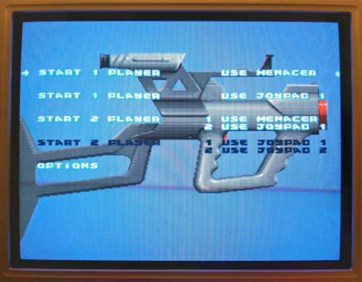
The Use Menacer options are white and selectable.
Somewhat unusually the Menacer's four buttons are mapped to the four data lines (instead of TL/TR) and are active high which means that if I start the game and let go of one of the Master System controller's buttons then it thinks I've pressed one of the Menacer's buttons (for example, releasing the "down" button makes DATA1 go high and the game thinks I'm pulling the trigger). Of course, I can't aim in this mode as there's no light gun input but it's good to see something is working!
I assumed that if TH is normally used for device identification I would start experimenting with using that to determine when the adaptor should output all zeroes. Considering the buttons need to be inverted to active-high logic too I thought it best to use an AND gate on each button so that if TH is high (normal state) the button input would pass through to the data line, but if TH is low (detection state) the data line would be forced low. I wired this up with an AND gate and four push buttons and the game still detected a Menacer and pressing a button in-game would now fire the weapon. Seeing that this worked, I removed one of the four push buttons that was previously used for the trigger button and used the TL data line from the Light Phaser instead via an inverter:
In the diagram above the TL on the left comes from the Light Phaser and the connections on the right go to the Mega Drive.
I assumed that the Menacer would also use the console's TH input for the light sensor from the gun (similar to the Light Phaser) so tried wiring up the Light Phaser's TH output to the Mega Drive's TH input. Moving the gun around the screen moved the aiming cursor around. Unfortunately, the aim was pretty far off:

The blue cursor should be under the gun, which is touching the screen.
The game placed the aiming cursor a consistent distance left of where the gun really was aiming. I assumed this was due to the game expecting a delay between when the gun saw the light from the screen and it sending a pulse to the console – unlike a wired gun that can send the signal back to the console very quickly the wireless Menacer converts the detected light pulse into an IR pulse that then needs to be handled by the receiving unit plugged into the console. By the time the console sees this pulse it will have moved further along the current scanline (right), so the game software works backwards (left) to an earlier point on the scanline. As I'm using a wired gun that transmits the signal much more quickly this left offset causes the aim to be incorrect.
The solution to this is to introduce our own delay into the signal, which I did with a crude RC circuit:
As I'd previously used a NAND chip to invert the signal from the trigger button I used three more of its gates to implement the delay. The first gate buffers the signal as the gun's TH is a common emitter output, so either connected to ground or pulled high via a resistor. This buffered signal then charges or discharges a capacitor to ground via a resistor – this provides most of the delay, and in my testing a 220Ω resistor and 100nF capacitor provided better aim. The next two gates buffer the signal again before driving a transistor for a common emitter output – as the console is also driving the TH line as an output I didn't want to directly drive it from the adaptor circuit and so the transistor seemed safer and is how the Light Phaser works anyway.
This is a crude circuit and has its limitations (very short pulses could be dropped entirely rather than delayed, for example) but it does at least seem to greatly improve the aim:

The cursor now lines up with the point on the screen the gun is touching.
The game is now fairly playable, though there is one notable flaw with the circuit: pressing any button at the main menu screen causes the game to assume the gun has been disconnected, disabling the Menacer options:
The Use Menacer options are dark and no longer selectable.
Clearly using the TH signal alone to disable the buttons is insufficient, we must need to also output 0 when TH is high for full compatibility with the peripheral ID reading and the gun must use some other technique to enable or disable the button data.
Fortunately, a copy of the Menacer patent can be downloaded from the Sega Retro website where it can be studied to see if it provides any more clues for how the Menacer works. It goes into some detail about how the gun communicates with the console, including this figure showing the gun:
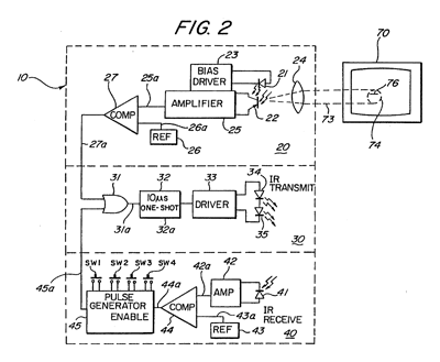
The centre portion of the image shows that infra-red signals from the gun are transmitted to the receiver in the form of 10µs pulses. The top portion of the image shows that these pulses can be generated by the gun's light sensor, so whenever the gun sees light it will send a 10µs IR pulse to the receiver. The bottom portion of the image shows the pulse generator used to encode the button presses; the button state is interpreted as a binary number and a corresponding number of IR pulses are sent: if SW1 is pressed then 1 pulse is sent, if SW2 is pressed then 2 pulses are sent, if SW3 is pressed then 4 pulses are sent and if SW4 is pressed then 8 pulses are sent. If multiple buttons are pressed then their values are added, so if SW1 (1) and SW3 (4) were pressed then five pulses would be sent up to a maximum of 15 pulses for all four buttons being pressed.
These button press pulses are only sent back to the console receiver after the gun receives an IR pulse from the receiver.
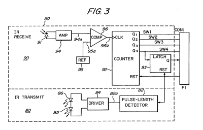
The receiver uses a counter chip to convert the IR pulses from the gun into button press or detected light pulses for the console. The duration of reset pulses are important here. The patent describes a standard counter reset pulse as being 2-3µs long and a main reset signal pulse as being about 10µs long. Any short reset pulse will reset the counter chip and latch. A long reset pulse will stil reset them, but also trigger a pulse of IR via the transmitter section at the bottom of the diagram. This IR pulse will cause the gun to send its button data back to the receiver, where the pulses will be counted by the counter chip and drive the DATA0 to DATA3 pins. After a certain delay to ensure that all button states have been sent the game software can read the button state and reset the counter, ready to read pulses from the light sensor in the gun. Bear in mind that the button state will have to be read before the active display starts, as the gun always sends an IR pulse when it sees light and this will cause the button presses to be miscounted.
Rather than pass every single detected pulse of light from the gun to the console it looks like the counter is used to detect eight pulses, after which it triggers a latch. This appears to be due to the assumption that when the gun is an expected distance away from the TV it will trigger on around 20 scanlines, and so by waiting for eight it will place the detected position roughly in the middle of those 20 lines.
All in all, this is a simple enough system but what does it mean for our convertor circuit? Will we need to add extra pulse length detectors and counters to make sure we send through the right sort of data?
I captured the state of the controller port lines during gameplay and found the above logic traces. Each frame TL goes high briefly and is then low for the active part of the frame. Pin TR has very brief pulses, and these appear to be the reset pulses. If we zoom in, we can see these more clearly:
Here TR goes high for over 10µs and so must be the main reset pulse (used to read the button state) and the next pulse is around 3µs and so must be the regular counter reset pulse. The gap between these pulses is only 85µs, however – if the button IR pulses are 10µs long then this would not give us enough time to read them – even if there was no gap between them 15 pulses of 10µs would take 150µs. Either there is a delay of at least 85µs before the gun starts sending the button data or the timing is different in the real gun when compared to the patent information. There is a final 3µs reset pulse as TL falls and this pulse comes 1.435ms after the previous short reset pulse so that would provide plenty of time to receive the button press data before resetting the counter ready to detect light pulses.
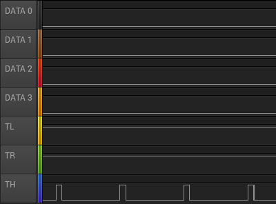
The next bit of the puzzle is what happens during the main menu when the Menacer is being detected. The traces are shown above. Both TL and TR are fixed high during this process. If we assume TR alone is used to reset the counters then holding this high would fix the data lines at %0000, identifying the controller as a Menacer. The TH line is also being pulsed here, possibly as the code is still checking to see if it could be some other type of controller.
If we force the output of the data lines to be 0 when TR is high (acting as a reset) then maybe this would work more reliably (and correctly) than when TH is low. I'll need to perform some further experiments, and also see whether the lack of the eight scanline delay before triggering the TH line to indicate detected light causes any other problems. I like the idea of a simple device that only uses logic chips to adapt the gun but if we need a more sophisticated circuit to time reset pulses and offset the vertical position maybe it would be better to switch to a microcontroller circuit. If that was the case, maybe the adaptor could also be programmed to work with games that use the Konami Justifier, another Mega Drive light gun that is incompatible with the Menacer.
If you'd like to see the circuit in action, I've uploaded a quick video on YouTube to accompany this post.
Modifying a Master System cartridge for use with flash ROMs
Thursday, 22nd August 2019
I have a ToToTEK GG-PRO flash cartridge to run homebrew software on my Game Gear however I have never been able to get it to work on my current PC and it seems that it's hard to find a Master System equivalent these days. A contemporary alternative is the Master EverDrive and it is by all accounts an excellent piece of equipment however it is a very expensive product.
I had, however, heard that certain Master System cartridges could be modified to accommodate a flash memory chip in place of their stock mask ROM. I do say certain cartridges as it's the ones with separate mapper chips that need to be used. One such cartridge is After Burner, and as I was able to find an inexpensive loose copy on eBay I used that as the basis of my modifications.
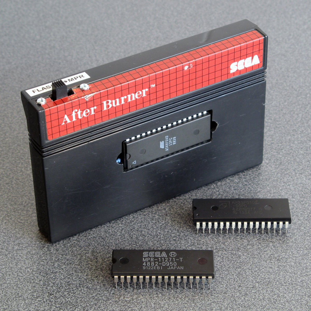
The memory mapper is used to map ROM banks or save RAM on the cartridge into one of three 16KB slots in the Z80's address space. Most Master System cartridges only contain a single chip that combines the ROM data for the game as well as the memory mapper logic. As such, these cartridges can't be modified for use with a generic flash memory chip as you can't access that internal memory mapper. Some cartridges, however, make use of a separate mapper chip and so you can remove the plain mask ROM chip and replace it with a flash memory chip. SMS Power! has this list of mappers and examples of cartridges in which they can be found.
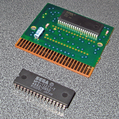
In the photo above you can see where I removed the mask ROM from the cartridge PCB and have left the mapper chip on the board. I didn't want to damage the old ROM chip (in case I wanted to play After Burner again) so I carefully unsoldered it rather than cutting it off the board. To do so I heated up each solder joint on the back of the board and used my spring-loaded solder sucker to remove the molten solder. After this I checked each pin by gently trying to move it in its hole; if it moved I knew it had been unsoldered and if it was stuck fast I knew I needed to try removing more solder. Once all pins were free the old ROM lifted cleanly out of the PCB.
One of convenient features of these cartridges is that the pinout of Sega's mask ROMs is virtually identical to the pinout of commonly-available flash memories like the 29F010 or 49F040. Only two pins need to be changed, as per the information on Charles MacDonald's website:
| Pin | Mask ROM | Flash memory |
|---|---|---|
| 1 | Not connected | A18 |
| 31 | A18 | /WE (Write Enable) |
As I wanted to ensure that the cartridge was compatible with both the original mask ROM and the replacement flash memory chip I thought it best to install a switch to let me select the type of memory that is installed. To break the connection between the solder pad on the PCB and the leg on the memory chip I used an IC socket with legs 1 and 31 bent out and not soldered through their corresponding holes. Wires are soldered to the bent out legs and go via the switch to the corresponding solder pads on the bottom of the PCB.
The position of A18 definitely needed to be swapped between pin 31 on the mask ROM and pin 1 on the flash memory if I wanted to be able to address all 512KB of a 4 megabit ROM. I had heard reports that the write enable pin on the flash memory can be left disconnected however the datasheets for the flash memory chips I checked did seem to indicate that it should be held high during read operations so I thought it best to hold it high when in "flash" mode. This means that the function of both pins needed to be changed by the switch, so I used a DPDT to make this happen. The two different states are illustrated below, showing the connections to the six pins on the bottom of the switch:
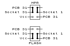
The heavy black lines show the position of the switch contacts when in the upper and lower positions. When in "MPR" mode you can see that pin 31 of the IC socket (A18) is connected to pin 31 of the PCB and pin 1 (NC) of the IC socket is not connected to anything. When in "FLASH" mode pin 31 of the IC socket (now /WE) is connected to Vcc and pin 1 of the IC socket (now A18) is connected to pin 31 of the PCB.
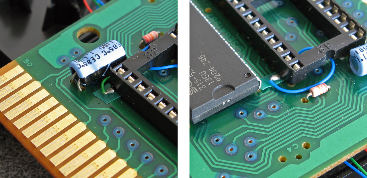
The photos above show how the pins of the IC socket were bent outwards with very fine wires soldered to them. These fine wires run through holes on the PCB under the IC socket to the underside. I did stick very small pieces of electrical insulating tape under the points where the solder joints for the wires attached to the bent pins made contact with the PCB for a bit of added security. With those legs bent out and the wires threaded through the PCB the socket could be soldered down.
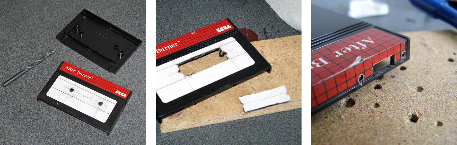
Unfortunately, one problem with using an IC socket is that the extra height means that the PCB no longer fits inside the cartridge shell. I needed to cut a rectangular hole in the cartridge enclosure for the chip to protrude through. I started by drilling two large round holes at the far ends of the chip - this allows me to use a chip puller (or small screwdriver) to pull (or lever) the chip out of the socket without needing to dismantle the cartridge each time. Due to the position of an internal support post very near to the memory chip a larger rectangular slot could not be cut – and I think this looks pretty neat anyway! A smaller rectangular hole was cut in the top of the cartridge shell for the switch to protrude through along with mounting holes for its two screws.
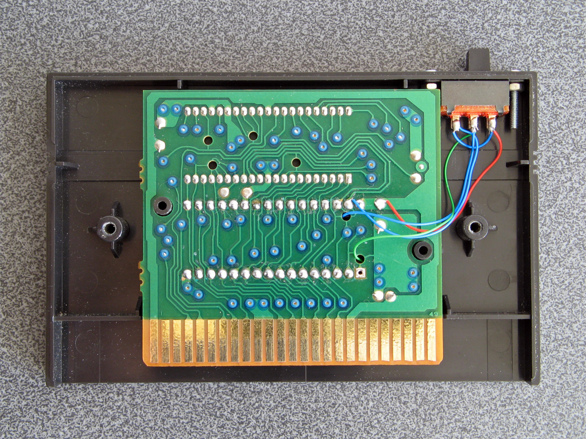
Here the switch has been mounted inside the case with the wires from the IC socket soldered to the appropriate pins on the switch and other wires connected to the appropriate pads on the back of the back of the PCB.
Inserting the original mask ROM for After Burner and setting the switch to MPR mode lets me play After Burner; writing a ROM image to a flash memory chip and inserting that with the switch set to FLASH mode let me run that program instead. Putting the switch on the wrong mode would take me to the console's built-in game of Hang On as the BIOS is no longer able to read the cartridge as a valid Master System game (at least when using a 512KB memory that requires A18 to be connected to the right pin). All in all I'm now happy that I have a way to run programs on my Master System from flash memory and do some homebrew experiments of my own on real hardware.
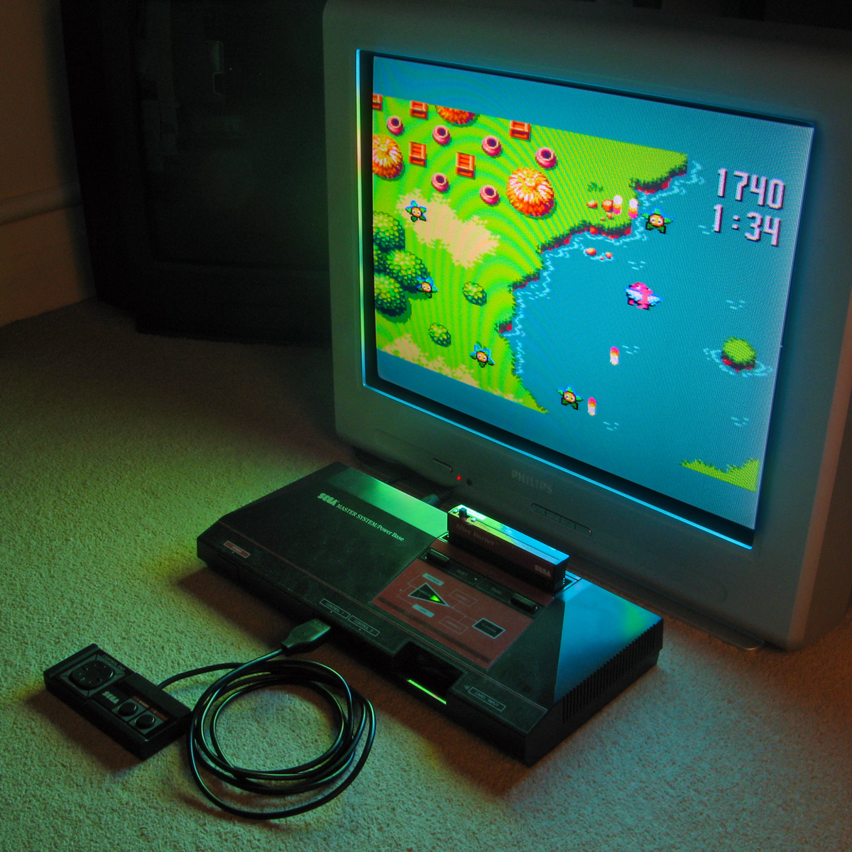
The above photo shows the excellent homebrew Flight of Pigarus by Kagesan running on my Master System courtesy of the modified cartridge. I've tested it so far with an AM29F010B (128KB/1 megabit) and an AT49F040 (512KB/4 megabit) and have been using the Willem programmer (along with Remapped IO.DLL to get it to work with my PC's PCI parallel port) to program the chips.
Updating remapped IO.DLL: The venerable Willem programmer still works on 64-bit Windows 10!
Sunday, 18th August 2019
A few years ago I posted about a way to get the Willem chip programmer to work with modern PCI parallel ports via a DLL that remapped the legacy port addresses to the ones of your modern card (in my case my card is installed at 0xCCD8 instead of 0x378). Since its release I've had several people contact me asking for advice and support, including a few questions about 64-bit support.
Until recently I had been using a 32-bit OS and as such hadn't run into compatibility issues myself. I had replaced the DLL in the zip archive for the project with an allegedly 64-bit-compatible version of the inpout32.dll library that the is used to access the I/O ports but I was unable to test this myself, however it still worked in a 32-bit OS so hoped that it would also work on a 64-bit OS as claimed.
I am now running a 64-bit OS and found myself needing to program a chip with my Willem programmer but was unable to do so, receiving the dreaded Hardware Error: Check Power & connection message. Clearly this DLL was not working as it should under 64-bit Windows!
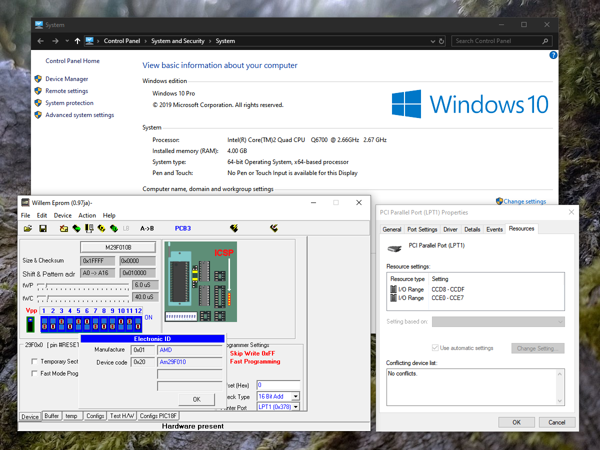
Fortunately, Phil Gibbons of highrez.co.uk has come to the rescue with a 64-bit compatible version of InpOut32 that works perfectly on my 64-bit Windows 10 machine as a drop-in replacement for the old library. I have updated the zip archive containing the software with the working library. For more details and a copy of the Willem programming software please see the Remapped IO.DLL project page.
A temporary solution for 3D games on the Master System without the 3D glasses adaptor
Monday, 29th July 2019
I bought my Sega Master System-compatible 3D glasses almost exactly ten years ago for use in my LCD Shutter Glasses Adaptor project.
More recently I've acquired a CRT television and an actual Sega Master System so I could in theory make use of the glasses as I had originally intended - with Sega Master System games.
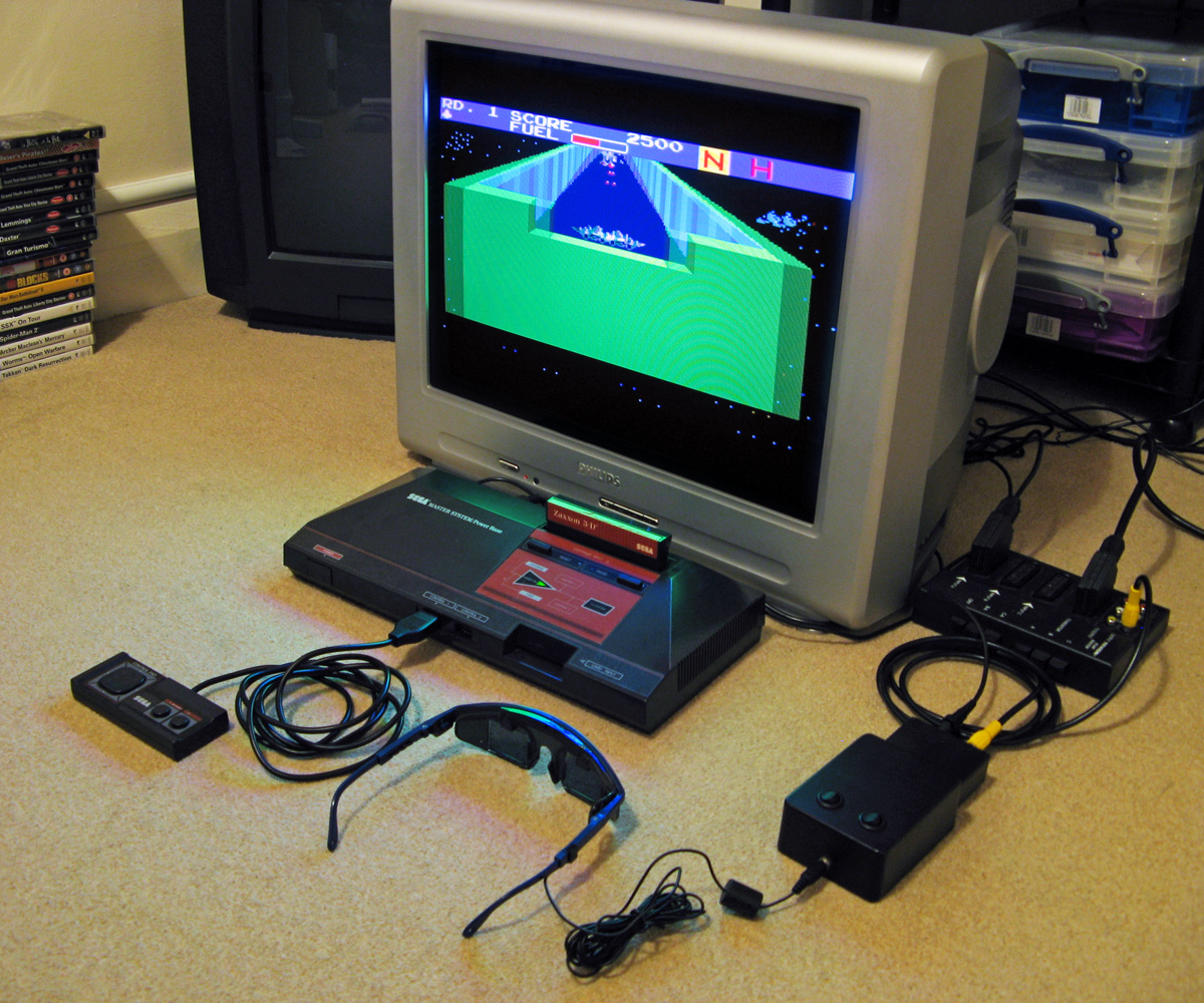
I've been keeping an eye on eBay for the 3D Glasses Adaptor for the Master System. This is a device that plugs into the console's card slot and allows it to drive the glasses with the software controlling which LCD shutter is open and which is closed by writing to the card. Unfortunately, these cards are not too easy to find in the UK and when they do appear they usually came bundled with a broken pair of glasses (it seems very unusual for both arms to still be attached to the glasses, and I've seen a fair few pairs that are cracked down the middle too). I already own some compatible 3D glasses so didn't want to waste money on buying a broken set of original Master System ones!
I did eventually find someone selling a loose adaptor for a reasonable price so bought it and a few games. Zaxxon 3-D was the first to arrive and I was eager to test it out. Without the card adaptor I needed to find an alternative solution, so my thoughts turned to the LCD Shutter Glasses Adaptor I'd built a few years ago.
This is designed to sit between a PC and a VGA CRT monitor and drives the shutter glasses, alternating which LCD shutter is open and which is closed every vertical sync. It can also blank out alternate scanlines, simulating an interlaced signal from a progressive one by blanking odd scanlines on one frame and even scanlines on the next, but this is not useful in our case. The Master System is already alternating complete left and right eye views on its own, so we just need to catch its equivalent of a vsync pulse and feed that into the VGA port on the back of the shutter glasses adaptor.
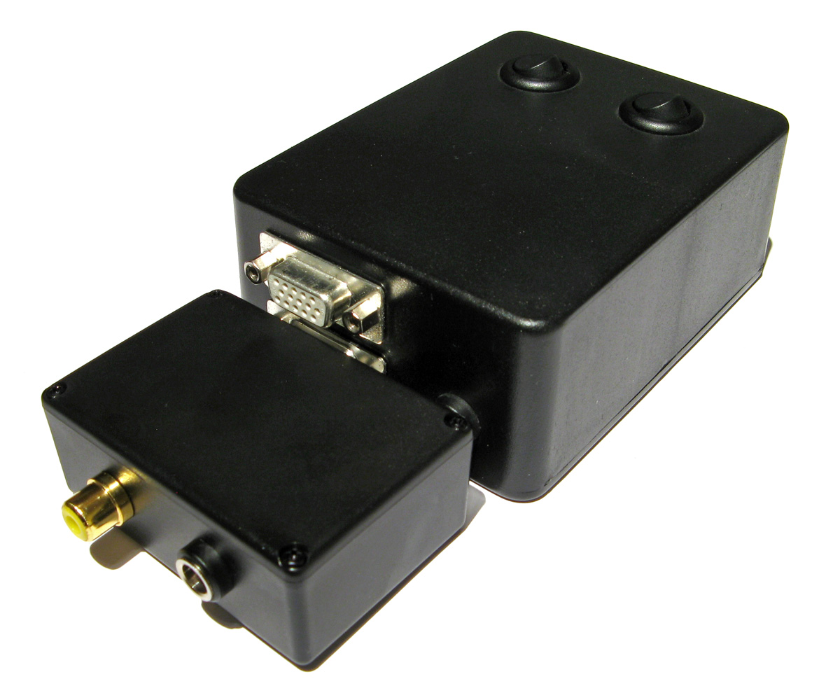
Above is the device I built, attached to the existing 3D glasses adaptor. It has a single composite input which should be connected to the composite output from the console, either via a splitter (if the console is connected to the TV using composite video) or via some sort of SCART breakout box (I'm using the composite video output from my SCART switch box). It also has a power socket which is used to power the circuit inside which is also passed through to the LCD shutter glasses adaptor. The box has a DE-15 connector and 5.5x2.1mm barrel plug on the other side for connections:
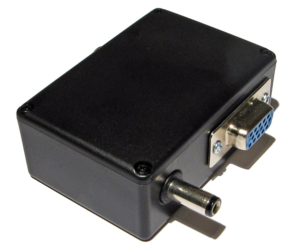
I'd cut the barrel plug off a faulty power supply years ago, I'm glad I kept it as it made the project a much neater solution than it might have other been!
The circuit inside is very simple indeed. As the original adaptor has its own 5V regulator inside and is designed to be powered from a 9V power supply I had to maintain the same convention for this device, so I use a 7805 regulator to convert the incoming voltage to 5V. This powers a textbook example of an LM1881 sync separator circuit - I'm using the reference circuit from the chip's datasheet, connecting the composite video input to the chip's composite video input via a 0.1µF capacitor (without termination as it's assumed the signal is being terminated by the TV) and I use the LM1881's composite sync output and vertical sync output for the VGA connector's horizontal and vertical sync connections respectively.

The circuit can be seen above, stuffed in the bottom of the box - along with copious amounts of hot glue to keep the barrel plug in place! How well does it work? Well, the below animation shows two views of the circuit in action, viewed through first one shutter and then the other of the 3D glasses:
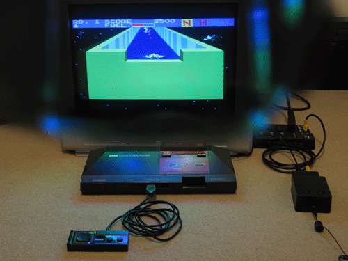
This isn't a perfect solution - the Master System expects to be able to explicitly specify which shutter is open whereas in our case we're simply be alternating every frame. This could mean that the eyes are swapped, however there is an eye swap switch on the shutter glasses adaptor to compensate. If the view looks wrong then the switch can be used to correct it, and once that's done as long as the software alternates the views every frame then it should be fine.
I'm certainly happy for now, as it lets me play my 3D games whilst waiting for the console's intended 3D glasses adaptor to arrive in the post.
Fixing the Dreamcast Race Controller's dead zone with a simple microcontroller circuit
Tuesday, 21st May 2019
I recently bought myself a Race Controller wheel for the Sega Dreamcast and was a little disappointed with the way that it performed. I had read reviews online before buying it and some did mention that it didn't handle particularly well but others did mention that it was about the best controller available for the system so I didn't feel it was too risky a purchase.
The issues I have with the wheel stem from its excessively large dead zone – you need to turn the wheel quite far before your car starts to turn, making it feel sluggish and unresponsive.
Fortunately, the wheel hardware is very simple internally – a 100KΩ potentiometer is used to detect the wheel's position and it outputs an analogue voltage to the controller PCB. We can take advantage of that to insert our own circuit between the potentiometer and controller PCB to sample the wheel position, add an large offset to it to push it outside the dead zone and then output that corrected voltage to the stock PCB. This will then cancel out the offset as part of the large dead zone before sending the position to the console.
The video above goes into more detail about how this circuit works as well as illustrating the problem with the stock dead zone. For more information and to download the code and circuit diagram please see the De-Dead Zone product page.
Repairing a PlayStation controller to USB adaptor
Saturday, 20th April 2013
I recently purchased an inexpensive PlayStation controller USB adaptor for my PC. Several reviews confirmed that it was compatible with the controller's analogue joysticks so I thought it would be what I was after. Life is rarely that easy with cheap electronics, unfortunately!

When it arrived I plugged it in and Windows installed the appropriate HID drivers for it automatically, but as much as I waggled the joysticks on a connected DualShock 2 controller the axis preview in Control Panel remained resolutely in the zero position. PlayStation controllers have an "Analog" button that can be pressed to toggle between digital and analogue modes, but any attempts to press this resulted in the "Analog" light briefly flashing before immediately switching off again.
Thinking it may be a driver issue I tried to install the drivers from the mini CD that had been included with the adaptor. My PC could not read the disc (it appeared to be scratched, and was not very well protected in postage) so I hunted around online until I found a package that worked using the device's USB ID (VID_0810&PID_0001). This enabled the controller's rumble/vibration feature, but I still couldn't get analogue input to work. Thinking that if one driver package could add vibration support, another might add analogue support I contacted the Amazon seller to ask them if they could send me a copy of the correct drivers - they instead chose to send me a whole other unit in the post.
In the meantime, I experimented with another controller plugged into the adaptor. I was surprised to find that with two controllers plugged in at once I could enable analogue mode on one of the controllers. This made me think there could be a power issue - the second controller increased the capacitance across the power supply, which would make it more resilient to voltage spikes and reduce ripple that could be causing the controller to reset out of analogue mode. This was further confirmed by plugging the adaptor with a single controller into a powered USB hub - in this scenario the controller would only leave analogue mode when vibrating. I checked the power supply pins on the controller ports and was very surprised to see that there was apparently nothing connected to pin 5, which is supposed to deliver +5V to the controllers. At this point I decided to dismantle the adaptor to see what was going on.
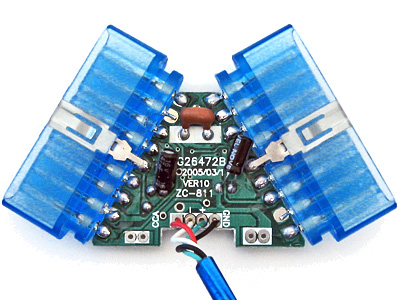
On the inside of the adaptor I could see that several components had been omitted. This could be to blame on cost-cutting measures (e.g. the LEDs D1 and D2 which are purely cosmetic) but the removal of D3 puzzled me the most - this diode is connected between USB VCC and the controller port pin 5, and is presumably responsible for providing power to the connected controller. I put this down to an oversight at the factory, and soldered a 1N4001 rectifier diode in the marked place.
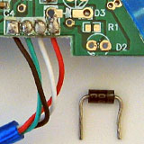
The above image shows a close-up of the place the missing diode should appear - D3 is indicated by a silk-screened diode symbol. Unsurprisingly the 1N4001 silicon diode has far superior characteristics to the silk-screen diode it replaced.
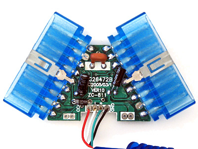
With the diode in place both controller ports started working flawlessly, even allowing me to use a wireless Guitar Hero controller receiver (though not the whammy bar - Guitar Hero controllers lack the "Analog" button to manually enable the analogue mode and instead rely on the PlayStation to enable it via software). Whilst I had the soldering iron out I thought I should add the missing LEDs, once again using the existing markings to establish the correct polarity:
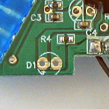
If the markings are unclear, the anode (+) is always to the left when viewing the bottom of the circuit board when the other markings are upright.
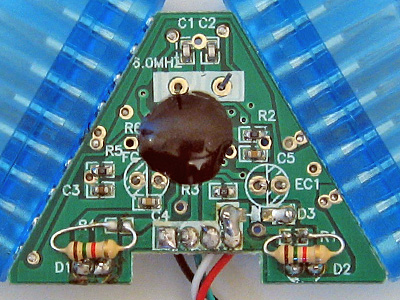
As the enclosure is blue and I seem to remember some fuss being made of the PlayStation 2's blue LED when it first came out I opted to use two blue LEDs with 1K5 resistors. I do not have any surface-mount resistors but through-hole ones fit quite easily though they can be a little fiddly to solder down.
When the replacement adaptor arrived in the post I was surprised to see that (once again) the diode D3 was missing and it demonstrated the same problems as the other one I'd fixed. I find it unlikely that the same mistake could be made twice, so this seems to be a genuine cost-cutting measure. Microcontroller I/O pins often have an internal protection diode between them and the positive power supply, which is how I assume the circuit works at all when the controllers are left unpowered - a small amount of current flows from the I/O (data) pins to the positive rail via these protection diodes, which is just enough to let the controller work in digital mode but once they draw more current (e.g. when sampling analogue inputs or driving the vibration motors) the voltage droops far enough for the controller to reset and leave analogue mode.
With these fixes in place I now have two working PlayStation USB adaptors for the price of one (and two 1N4001 diodes). I'm still rather perplexed by why there's such a blatent flaw in the hardware, but it is at least an easy fix which is why I've written it up. In summary: if your cheap PlayStation to USB adaptor ("Twin USB Vibration Gamepad", "Twin USB Joystick") is not working correctly, unscrew it and see if D3 is missing. If it is, solder a 1N4001 or similar diode between the two holes left for that purpose.
TV Demonstrator for TI calculators
Monday, 11th October 2010
I've been tinkering with a number of small projects recently. I've resumed work on an LED clock for my bedroom (using a 32×8 LED display) and written an experimental BASIC interpreter in C# which I may try to turn into an assembler (implementing assembly statements as BASIC ones). In the mean time, I have finished one project — a device to display a calculator's screen on a television set.
Texas Instruments also manufacture a product that allows you to view the screen contents of a calculator with supported hardware on a TV; here is a video demonstrating it. The additional hardware (either on special "ViewScreen" calculator models or built into the more advanced calculators such as the TI-84+) allows the device to mirror what is sent to the calculator's LCD in real-time.
I do not have one of these calculators, just a plain old TI-83+. However, this calculator (as well as the older TI-83 and TI-82) allows you to capture a screenshot over the link port. Pressing a button on my device captures a screenshot in this manner and displays it on the TV. This relies on the calculator being in a state where it can respond to these screenshot requests, so is not ideal, but considering that the TI Presenter costs $300 and relies on special hardware inside the calculator and mine should cost less than a tenth of that in parts and work with older calculators I think it's a decent compromise.
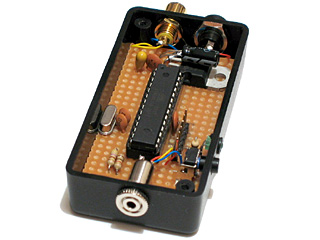
I had previously believed that NTSC composite video signals used a negative voltage for sync pulses. I have since found documents that indicate that the sync, black and white levels are the same as those for PAL. The timing is, naturally, different but as there's no need to change the hardware it makes supporting both NTSC and PAL relatively straightforwards. This contraption can be set to operate in either NTSC or PAL mode by sending the real variable M to it from the calculator, with a value of 60 for NTSC and 50 for PAL.
I acknowledge that this is not the most useful of projects (unless you're a maths teacher with an interest in electronics) but the code may be of interest for other projects. A handful of inexpensive parts can get you a picture on a TV from a 96×64 monochromatic frame buffer (the 1KB RAM on the ATmega168 doesn't allow for much more, alas).
More information and downloads can be found on the TV Demonstrator project page.
Integrating the dsPIC33 VDC with the Z80 computer
Saturday, 31st July 2010
The ultimate goal for the video display controller module I have been working on is to drive the display in my Z80 computer project. As I have now got a pretty good set of features I thought it would be a good idea to join the two projects together.
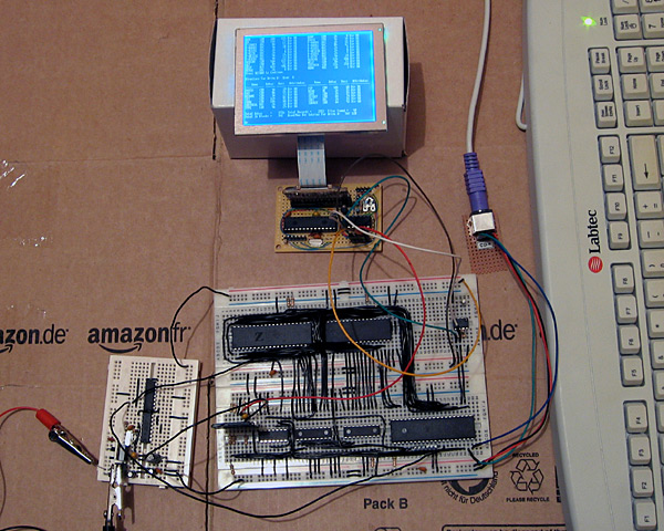
The big board in the lower middle of the above photograph is the main body of the computer, including the Z80, its RAM, the ATmega644P that is used to handle I/O, an SD card for storage and a DS1307 real-time clock. The small board in the bottom left of the photo is the power supply (supplying both 5V and 3.3V) and clock generator (providing a 20MHz and 10MHz clock).
At the top of the photo is the video display controller, connected to a 320×240 graphical LCD. A pin header is used to connect this VDC board to the rest of the computer. Three pins are required for power; 0V, 3.3V (dsPIC33 and output buffer) and 5V (LCD). The VDC is connected to the computer's ATmega644P I/O controller using the two-wire I2C bus (the same bus that is used to access the DS1307 clock). Rather than run a series of graphical demos, the VDC now waits for commands to be written to the I2C slave address 0xEE which it acts on to control what is shown on the screen. I'm aiming for these commands to work in the roughly same way as they did on the BBC Micro VDU, which should make porting the enhanced TI-83+ version of BBC BASIC to this computer a bit easier. The BBC Micro's VDU could be accessed by calling OSWRCH (assuming it was being used as the current output stream), which typically has an address of &FFEE — hence my choice of 0xEE as the I2C slave address!
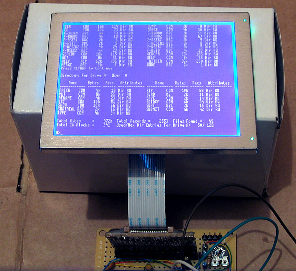
A handful of these VDU commands have been implemented, which is sufficient to run simple CP/M software. The generic CP/M version of BBC BASIC does not, naturally, support any hardware-specific features and as such lacks advanced text or drawing support (one can send commands directly to the output stream with the VDU statement but this isn't very user-friendly). I will need to work on this now that the hardware is coming together! The current VDC code can be downloaded here if you are interested in the changes that have been made.
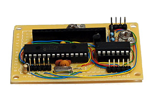
The above photo shows the newly constructed VDC hardware. All of my previous projects have been assembled on stripboard; as the projects have become more complex or simply smaller I've found stripboard to be increasingly awkward to work with. ICs can only really be orientated in one direction, and to reduce the size of circuits I've had to start cutting the tracks between holes (rather than the usual method which is to drill out an entire hole). The supplier I normally acquire parts from, Bitsbox, recently added three different sizes of perfboard to their catalogue so I thought I'd give it a go. I've found it much more pleasant to work with than stripboard, though not as easy to correct if you make a mistake and need to desolder a connection. You can certainly perform some interesting space-saving tricks on the underside of the board!
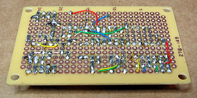
The Kynar insulation on the wire I switched to using also has the advantage of not melting when heated with a soldering iron, as I've had problems in previous projects where tightly-spaced wires will end up getting shorted together as the insulation between them melts.
I have mentioned that one pin header is used to connect the VDC to the computer. There are three others on the board; the two-pin one is for the composite video output, the six-pin one is for connection to a PICkit to reprogram the dsPIC and the four-pin one for the VGA output.
Now that I have moved the VDC onto a permanent circuit board I feel that I can start moving the rest of the computer in the same direction. The software is far from complete and the hardware is pretty rudimentary but it does basically work and having a more robust system to work on should make life a bit easier.
VGA output for the dsPIC33 VDC
Sunday, 25th July 2010
I have spent quite a while working on different projects that generate PAL video signals in software. This may seem a bit odd if you consider the fact that I don't own a TV, so tend to rely on a video capture card or VGA box to see the output of these projects on a computer monitor — something I do have a fair number of.
This reliance on another piece of technology between my project and the display device is not something I'm too keen on, so have spent some time adding native 640×480 60Hz VGA output to my dsPIC33 video display controller.
Another advantage of using a VGA monitor directly is that individual pixels are shown very crisply, unlike my video capture card or VGA box which tend to blur the image horizontally. This is shown in the zoomed in part of the above photo.
Generating a video signal for a VGA monitor is easier than generating a composite video signal for a PAL TV, as there are distinct pins for the image data, horizontal sync and vertical sync. One problem I did have, however, is with the length of the vertical sync pulse. I started with a very brief pulse (the same duration as the horizontal sync pulse) which worked fine with my old analogue CRT monitors but didn't work at all with my modern LCD monitor. The documentation I was using for timing information indicated that there were "two scanlines" for vertical sync so I extended the pulse to last for those two frames, which worked on the LCD but didn't on the CRTs. My final compromise has been to assert the vertical sync pin for the duration of a single scanline, which seems to work on all of my monitors.
When connected to a TV two microcontroller pins are used to drive a single load (composite input). When connected to a VGA monitor, however, a single microcontroller pin is used to drive three loads (red, green and blue inputs). I thought it prudent to check the datasheet for the dsPIC before connecting this increased load to the output pin where I was surprised to discover that the maximum source or sink current for each output pin is a measly 4mA — not even enough to drive an LED! I have added a buffer to each video output pin to protect the dsPIC — any buffer capable of sourcing up to 30mA or so should be sufficient (I'm using a 74F125, which can be seen in the bottom right of the above photo). I had previously been occasionally using the video output pins as inputs to check if there is a load on the output or not (such a load would indicate whether a TV or VGA monitor is plugged in or not) but I can no longer do this with the external buffer IC so have had to revise the circuit somewhat. Updated source code featuring the new VGA output code and an accompanying schematic are available for those who are interested!
Text and filled shapes for the dsPIC33 VDC
Thursday, 22nd July 2010
The dsPIC33 video display controller project I am working on needs to support several common text output and drawing operations offered by existing BBC BASIC implementations. The previous demo included basic point, line and circle outlining functions, but I also need to output text and outline (or fill) rectangles, circles, ellipses and triangles. On top of that the drawing operations need to support multiple colours and plotting modes. Owing to processing power and memory limitations the output is black and white only but different "shades" can be implemented with dither patterns. The plotting modes allow you to perform logical operations between what you are drawing and what's currently on the buffer — for example, you could fill a circle that is logically ORed with the existing background or draw a line that inverts every pixel along its length rather than applying the new colour.
Filled rectangles and text output produce the above image.
Finding suitable algorithms for some of these routines has been a little tricky at times. Due to the way that filled shapes can be set to invert (rather than overwrite) what's on the background there has to be zero overdraw and the outline of filled triangles should exactly match the outline of a triangle drawn by plotting a line between its three vertices; this makes combining triangles to form more complex shapes possible, as you can guarantee that the overlap between the two shared vertices of a pair of triangles covers the same pixels as a line drawn between those two vertices.

Filled triangles produce a solid cube.
I ended up writing a program in C# that would plot a random triangle using the triangle filler I was attempting to write and then compare its outline to that of a triangle drawn by plotting lines between the three vertices. The final code is chock full of special cases and workarounds but has been tested against hundreds of thousands of random triangles and seems to be working!
Due to a shortage of memory there is only a single frame buffer, which (naturally) means there is no double-buffering and hence smooth animation becomes a little tricky. When connected to a TV one can take advantage of the vertical blanking period to update the buffer (this is a period below and above the active display where you only need to feed sync signals, not image data, to the TV) and still get decent effects as long as you don't try to do too much. The LCD has no such vertical blanking period and so some of the demos look rather flickery.

I have captured a video of the output of the circuit when running the demo which can be seen above. The horizontal grey lines are a limitation of my video capture card; these lines appear correctly as alternating black and white pixels on a real TV set! You can download the code for this demo from my site along with a PDF of the schematic. As this is a work in progress I'm sure there are plenty of bugs left to squash but I think it's getting there, slowly but surely!
360 degree photos from Lego, a PICAXE, C# and JavaScript
Friday, 9th July 2010
As you may have guessed from the ratio of photos to actual content in my entries I do quite enjoy taking photos of things. One of the reasons I enjoy working with electronics over writing software for computers is that a finished product results in something physical, which I find much more rewarding than a purely virtual hobby.
One type of photograph I particularly enjoy on other websites is the interactive 360° view of a product. The ability to click and drag to rotate an object on the screen makes it seem more real.
What do you need to take this sort of photograph and show it on a web page? There are four components I could think of:
- A rotating platform that could be controlled to rotate to a specific angle.
- A fixed camera that can be triggered once the platform has advanced to the correct angle.
- A way to combine all of the photos taken at different angles into a single file.
- An piece of code that would allow the user to rotate the object on-screen and display the correct single view of the object.
My final solution is a bit of a Heath Robinson affair but it seems to work quite well!
The rotating platform
The most obvious way to build such a platform is to use a stepper motor, as that is specifically designed to be positioned to a particular angle. The problem is that I don't have any stepper motors, and even if I did it would be quite tricky to connect one to a platform. A more practical alternative is to use something I do have — Lego Technic.
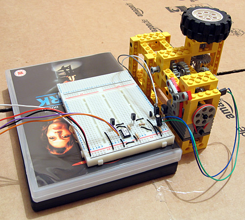
A Lego motor cannot be set to rotate to a particular position, so some additional electronics are required. The motor drives a worm gear which in turn rotates a three-bladed propeller relatively slowly (shown with red pieces attached to it in the photo). This propeller cuts the path of a beam of infra-red light between an LED and an infra-red receiver module. A microcontroller (in this case, a PICAXE-08M) is used to advance the platform in steps by switching the motor on, waiting for the beam to be unblocked, waiting for the beam to be blocked again then switching the motor off. The gears I am using have twenty-four or eight teeth, so each pair of gears divides the rotational speed by 24/8=3. I am using four pairs of gears which results in a division of 34=81. The propeller has three blades which further divides the rotational speed by three resulting in the ability to set the platform to 81×3=243 distinct angles.
' This code is for a PICAXE-08M
#PICAXE 08M

' This pin is used to generate the 38kHz IR carrier. It should be connected to the IR LED's cathode (-).
Symbol IRPwmPin = 2
' This pin is connected to the IR demodulator's output.
Symbol IRReceiverPin = Pin3

' This pin is connected to the motor enable output.
Symbol MotorPin = 4

Symbol SerialControlIn = 1

' The desired position of the "stepper" motor.
Symbol StepDesired = B8
' The current position of the "stepper" motor.
Symbol StepCurrent = B9

Symbol StepDesiredConfirm = B10
Symbol StepDesiredPotential = B11

' Returned from the CheckBeam routine.
Symbol BeamBlocked = B12

' Rather than spin once at a time (slow) spin up to this many times between exchanging position information with the computer.
Symbol SpinLoopCount = 3

' Stores the spin loop time.
Symbol SpinLoop = B13

' The number of steps in a complete revolution.
Symbol TotalSteps = 243


Main:

    ' Reset the current and desired steps.
    StepDesired = 0
    StepCurrent = 0

    ' Switch the motor off.
    Low MotorPin

    'StepDesiredConfirmCount = 0

    Do
        ' Fetch the desired position.
        SetFreq M8
        SerIn SerialControlIn, N4800_8, (CR, LF), #StepDesiredPotential, #StepDesiredConfirm
        SetFreq M4

        ' Check the received data - the second value should be the logical inversion of the first.
        StepDesiredConfirm = Not StepDesiredConfirm
        If StepDesiredPotential = StepDesiredConfirm Then
            StepDesired = StepDesiredPotential
        End If


        ' Adjust the position if required.
        For SpinLoop = 1 To SpinLoopCount

            ' Broadcast the current step position.
            SerTxd(#StepCurrent, ",", #StepDesired, CR, LF)

            ' Do we need to run the motor?
            If StepCurrent <> StepDesired Then

                ' Switch the motor on.
                High MotorPin
                Pause 20

                ' Wait for the beam to be unblocked.
                Do GoSub CheckBeam
                Loop Until BeamBlocked = 0


                Pause 20

                ' Wait for the beam to become blocked again.
                Do GoSub CheckBeam
                Loop Until BeamBlocked = 1

                ' Switch the motor off.
                Low MotorPin

                ' Increment step current to indicate a change of step.
                Inc StepCurrent
                If StepCurrent = TotalSteps Then
                    StepCurrent = 0
                End If
            End If


        Next SpinLoop

    Loop

' Checks whether the beam is blocked or not.
' Returns BeamBlocked = 0 for an unblocked beam, BeamBlocked for a blocked beam.
CheckBeam:
    PwmOut IRPwmPin, 25, 53 ' 38kHz, calculated via PICAXE->Wizards->pwmout
    Pause 1
    BeamBlocked = IRReceiverPin
    PwmOut IRPwmPin, Off
    Return
The BASIC program on the PICAXE constantly outputs the current position and desired position via the serial programming cable as ASCII in the format <current>,<desired><CR><LF>. It also checks for the desired position every loop on via a serial input pin (sadly not the one used for programming the PICAXE as that is not permitted on the 08M) in the format <CR><LF><desired>,<~desired>. (again in ASCII). The desired position is transmitted twice, once normally and the second time inverted (all zero bits set to one and all one bits set to zero) as a simple form of error detection; should the second value received not be a logical inversion of the first then the value is discarded.
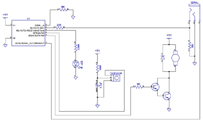
A copy of the schematic can be downloaded by clicking the above thumbnail. It is pretty simple; serial data is input on pin IN1 (move the serial input from the programming cable from SERIAL_IN to IN1), an IR LED is driven from pin PWM2 via a current-limiting resistor, an IR receiver sends its input to pin IN3, a Darlington pair drives the motor via pin OUT4 and information is sent out via the SERIAL_OUT pin (no need to move the programming cable for that one).
Triggering the camera
My camera does not have a standard remote control, but does has some software that allows you to capture shots when it's connected to your USB port. Unfortunately the Canon PowerShot SDK is rather old and is no longer maintained, which means that any software that uses it is bound to its bugs and limitations. One of its bigger problems is that it doesn't work on Vista; by setting the Remote Capture utility into XP compatibility mode I could set up a shot and see a live viewfinder but attempting to release the shutter caused the app to hang for about a minute before claiming the camera had been disconnected.
Fortunately VirtualBox emulates USB and serial ports so I set up Windows XP in a virtual machine and installed the Remote Capture utility. It still doesn't work very well (taking about thirty seconds between releasing the shutter and transferring the image) but it's better than nothing.
To control platform I use the following C# code. It's very poorly written (you need to make sure that you quickly set the Remote Capture application as the foreground window when you start it, for example, and it has a hard-coded 10 second delay after taking the photo to transfer the photo from the camera to the PC — when my camera's batteries started going flat it started to drop frames).
using System;
using System.Globalization;
using System.IO.Ports;
using System.Text;
using System.Text.RegularExpressions;
using System.Threading;
using System.Windows.Forms;
using System.Diagnostics;
using System.Linq;

class Program {

    const int StepsInRevolution = 243;

    enum ApplicationState {
        AligningStepper,
        WaitingStepperAligned,
        WaitingStartPistol,
        Photographing,
        Exiting,
    }

    static void Main(string[] args) {
        StringBuilder receivedData = new StringBuilder();
        using (var serialPort = new SerialPort("COM1", 4800, Parity.None, 8, StopBits.Two)) {
            serialPort.WriteTimeout = 1;

            serialPort.Open();

            var packetFieldsRegex = new Regex(@"^(\d+),(\d+)$");

            int? currentPosition = null;
            int desiredPosition = 0;
            int? confirmedDesiredPosition = null;
            int startPosition = 0;

            int angleCount = 64;
            int currentAngle = 0;

            serialPort.DataReceived += new SerialDataReceivedEventHandler((sender, e) => {
                if (e.EventType == SerialData.Chars) {
                    receivedData.Append(serialPort.ReadExisting());
                    string receivedDataString;
                    int newLinePosition;
                    while ((newLinePosition = (receivedDataString = receivedData.ToString()).IndexOf("\r\n")) != -1) {
                        var packet = receivedDataString.Substring(0, newLinePosition);
                        receivedData = receivedData.Remove(0, packet.Length + 2);
                        var packetFields = packetFieldsRegex.Matches(packet);
                        if (packetFields.Count == 1) {
                            currentPosition = int.Parse(packetFields[0].Groups[1].Value, CultureInfo.InvariantCulture);
                            confirmedDesiredPosition = int.Parse(packetFields[0].Groups[2].Value, CultureInfo.InvariantCulture);
                        }
                    }
                }
            });

            ApplicationState appState = ApplicationState.AligningStepper;

            // Main loop.
            while (appState != ApplicationState.Exiting) {
                // Update the stepper position.
                try {
                    serialPort.Write(string.Format(CultureInfo.InvariantCulture, "\r\n{0},{1}.", desiredPosition, (byte)~desiredPosition));
                } catch (TimeoutException) {
                    serialPort.DiscardOutBuffer();
                }
                Thread.Sleep(10);
                // What are we doing?
                switch (appState) {
                    case ApplicationState.AligningStepper:
                        if (currentPosition.HasValue) {
                            desiredPosition = (currentPosition.Value + 5) % StepsInRevolution;
                            appState = ApplicationState.WaitingStepperAligned;
                        }
                        break;
                    case ApplicationState.WaitingStepperAligned:
                        if (currentPosition.Value == desiredPosition) {
                            startPosition = desiredPosition;
                            appState = ApplicationState.WaitingStartPistol;
                            //while (Console.KeyAvailable) Console.ReadKey(true);
                            //Console.WriteLine("Press any key to start rotating...");
                        }
                        break;
                    case ApplicationState.WaitingStartPistol:
                        //while (Console.KeyAvailable) {
                        //  Console.ReadKey(true);
                            appState = ApplicationState.Photographing;
                        //}
                        break;
                    case ApplicationState.Photographing:
                        if (currentPosition == desiredPosition) {
                            Console.Write("Taking photo {0} of {1}...", currentAngle + 1, angleCount);
                            SendKeys.SendWait(" ");
                            Thread.Sleep(10000);
                            Console.WriteLine("Done!");
                            if (currentAngle++ == angleCount) {
                                appState = ApplicationState.Exiting;
                            } else {
                                desiredPosition = (startPosition + (currentAngle * StepsInRevolution) / angleCount) % StepsInRevolution;
                            }
                        }
                        break;
                }
            }

            Console.WriteLine("Done.");
            Console.ReadKey(true);
        }
    }
}
It was meant to prompt to press a key before starting to allow you to re-align the object to the starting position (if required) but this would switch focus away from the Remote Capture utility. I'll probably fix this to switch the focus explicitly to the Remote Capture utility before sending the key to trigger a capture, and will also add code that polls the photo destination directory to spot when the file has been downloaded from the camera instead of the hard-coded 10 second delay. Working in the virtual machine and with the buggy Remote Capture utility is a frustrating endeavour so I left it as it is for the time being!
Stitching the photos together
Once the photos had been taken they needed to be stitched together into a single file. I decided to use 64 angles for a complete revolution as this seemed a good trade-off between fine control over rotation and a decent file size. It also allowed the images to be arranged into a neat 8×8 grid.
I first used VirtualDub to crop each image. VirtualDub allows you to open an image sequence and export to an image sequence so it seemed ideal for the task. Once I had the object neatly cropped I stitched all of them together into a large single PNG file using the following C# program:
using System;
using System.Drawing;
using System.IO;
using System.Text.RegularExpressions;

class Program {
    static void Main(string[] args) {
        var middleImage = 14; // Index of the "middle" (default angle) image.
        var nameRegex = new Regex(@"Processed(\d{2})");
        var images = new Bitmap[64];
        try {
            foreach (var file in Directory.GetFiles(@"D:\Documents\Pictures\Digital Photos\Projects\Line Blanker\Insides 360\Processed", "*.png")) {
                var matches = nameRegex.Matches(file);
                if (matches.Count == 1) {
                    images[int.Parse(matches[0].Groups[1].Value)] = new Bitmap(file);
                }
            }
            var maxSize = new Size(0, 0);
            for (int i = 0; i < images.Length; i++) {
                if (images[i] == null) {
                    Console.WriteLine("Image {0} missing!", i);
                } else {
                    maxSize = new Size(Math.Max(images[i].Width, maxSize.Width), Math.Max(images[i].Height, maxSize.Height));
                }
            }
            using (var finalImage = new Bitmap(maxSize.Width * 8, maxSize.Height * 8)) {
                using (var g = Graphics.FromImage(finalImage)) {
                    g.PixelOffsetMode = System.Drawing.Drawing2D.PixelOffsetMode.Half;
                    for (int x = 0; x < 8; ++x) {
                        for (int y = 0; y < 8; ++y) {
                            var image = images[(x + y * 8 + middleImage) % images.Length];
                            if (image != null) {
                                g.DrawImage(image, new Point(x * maxSize.Width + (maxSize.Width - image.Width) / 2, y * maxSize.Height + (maxSize.Height - image.Height) / 2));
                            }
                        }
                    }
                }
                finalImage.Save("out.png");
            }
        } finally {
            for (int i = 0; i < images.Length; i++) {
                if (images[i] != null) {
                    images[i].Dispose();
                    images[i] = null;
                }
            }
        }
    }
}
The program requires that the input images are named Processed00.png to Processed63.png, which is easily arranged when exporting an image sequence from VirtualDub. The resulting image can be tidied up in a conventional image editor.
Embedding the result on a web page
The final bit of code required is to allow the 360° image to be embedded and manipulated on a web page. I opted to use JavaScript for this task as it seemed the lightest and simplest way to work.
if (typeof(Rotate360) == 'undefined') {
    var Rotate360 = new Class({
        Implements : [Options, Events],
        options : {
            width : 320,
            height : 240,
            container : null,
            element : null
        },
        sign : function(v) {
            return (v > 0) ? +1 : (v < 0 ? -1 : 0);
        },
        initialize : function(source, options) {
            this.setOptions(options);
            this.source = source;
            var rotate360 = this;
            this.element = new Element('div', {
                'class' : 'rotate360',
                styles : {
                    width : this.options.width + 'px',
                    height : this.options.height + 'px',
                    background : 'transparent no-repeat url("' + this.source + '") scroll 0 0'
                },
                events : {
                    mouseenter : function(e) {
                        if (typeof(rotate360.mouseHandlerDiv) != 'undefined') {
                            var myPosition = rotate360.element.getCoordinates();
                            rotate360.mouseHandlerDiv.setStyles({
                                left : myPosition.left + 'px',
                                top : myPosition.top + 'px',
                                width : myPosition.width + 'px',
                                height : myPosition.height + 'px'
                            });
                        }
                    }
                }
            });
            this.mouseHandlerDiv = new Element('div', {
                styles : {
                    position : 'absolute',
                    cursor : 'e-resize'
                },
                events : {
                    mousemove : function(e) {
                        if (typeof(rotate360.mouseHeld) != 'undefined' && rotate360.mouseHeld && typeof(rotate360.previousPageX) != 'undefined' && typeof(rotate360.previousPageY) != 'undefined') {
                            var currentBackgroundPosition = rotate360.element.getStyle('background-position').split(' ');
                            currentBackgroundPosition[0] = parseInt(currentBackgroundPosition[0]);
                            currentBackgroundPosition[1] = parseInt(currentBackgroundPosition[1]);
                            if (typeof(rotate360.rotateX) == 'undefined') rotate360.rotateX = 0;
                            rotate360.rotateX += (e.page.x - rotate360.previousPageX) / (360 * (rotate360.options.width / 270) / ((rotate360.image.width * rotate360.image.height) / (rotate360.options.width * rotate360.options.height)));
                            var workingAngle = parseInt(rotate360.rotateX);
                            currentBackgroundPosition[0] = -rotate360.options.width * (workingAngle % (rotate360.image.width / rotate360.options.width));
                            currentBackgroundPosition[1] = -rotate360.options.height * Math.floor(workingAngle / (rotate360.image.height / rotate360.options.height));
                            while (currentBackgroundPosition[0] > 0) currentBackgroundPosition[0] -= rotate360.image.width;
                            while (currentBackgroundPosition[0] <= -rotate360.image.width) currentBackgroundPosition[0] += rotate360.image.width;
                            while (currentBackgroundPosition[1] > 0) currentBackgroundPosition[1] -= rotate360.image.height;
                            while (currentBackgroundPosition[1] <= -rotate360.image.height) currentBackgroundPosition[1] += rotate360.image.height;
                            rotate360.element.setStyle('background-position', currentBackgroundPosition[0] + 'px ' + currentBackgroundPosition[1] + 'px');
                            rotate360.previousPageX = e.page.x;
                            rotate360.previousPageY = e.page.y;
                        } else {
                            rotate360.previousPageX = e.page.x;
                            rotate360.previousPageY = e.page.y;
                        }
                    },
                    mousedown : function(e) {
                        e.stop();
                        rotate360.mouseHeld = true;
                        rotate360.mouseHandlerDiv.setStyles({
                            left : 0,
                            width : '100%'
                        });
                    },
                    mouseup : function(e) {
                        e.stop();
                        rotate360.mouseHeld = false;
                        rotate360.element.fireEvent('mouseenter');
                    }
                }
            }).inject(document.body, 'top');
            this.image = new Asset.image(this.source, {
                onload : function() {
                    if (rotate360.options.element) {
                        rotate360.element.replaces(rotate360.options.element);
                    } else if (rotate360.options.container) {
                        rotate360.options.container.adopt(rotate360.element);
                    }
                }
            });
        }
    });
    window.addEvent('domready', function() {
        $$('img.rotate360').each(function(rotate360) {
            var src = rotate360.src.replace(/\.([a-zA-Z]+)$/, '_360.$1');
            var img = new Asset.image(src, {
                onload : function() {
                    new Rotate360(img.src, {
                        width : rotate360.width,
                        height : rotate360.height,
                        element : rotate360
                    });
                }
            });
        });
    });
}
The above code requires MooTools (both "core" and "more" for its Asset classes). It can be invoked manually or (preferably) will replace any image with a class of rotate360 with the 360° version — if the file was example.jpg the 360° version would be example_360.jpg.
Examples
I've taken photos of a few of my previous projects using this technique — USB remote control, AVR TV game and VGA line blanker. The process could use some refinement but it certainly seems to work!
dsPIC33 VDC with GLCD or PAL TV output
Sunday, 4th July 2010
I have currently been using some terminal emulation software on my PC to see the output of the Z80 computer. It seems a little silly to rely on a large multi-gigahertz, multi-megabyte machine just to display the output from a machine at the megahertz and kilobyte end of the scale. I had previously done some work with a dsPIC33 to drive a 320×240 pixel graphical LCD so dug out its breadboard and dusted off the code to try to make something of it.
Inspired by John Burton's recent experiments with PAL TV output I decided that the first thing I should do is add support for TV output. The graphical LCD is nice but a little small and responds to pixel changes rather slowly, making animation very blurry.

I think the results are reasonably good. A lot of the code is shared with the old LCD driving code, which means that the LCD demos work fine with the TV too. Fortunately, retracing the TV is a much less CPU-intensive job than retracing the LCD. The PIC has an SPI peripheral that allows you to clock out eight or sixteen bits a bit at a time at a selected speed by writing to a single register, which is great for clocking out the pixel data on each scanline. Even better are the PIC's DMA channels, which allow you to output a selected number of bytes or words to a selected peripheral from a specified location in RAM with no CPU involvement; all I need to do on each line is to copy a complete scanline to the DMA memory, initiate a transfer from this memory to the SPI peripheral and the job is as good as done. Using the DMA hardware as opposed to writing to the SPI registers directly reduced the rendering time of the Mandelbrot fractal part of the demo from 33 seconds to 18 seconds.
One problem I haven't been able to resolve is that the PIC inserts a small delay between every DMA/SPI transfer, which results in every sixteenth pixel being a bit wider than the fifteen before it. This is especially noticed on dithered regions. If I write to the SPI registers directly this delay vanishes. I'm not sure if the picture quality increase is worth the loss of performance, so I'd rather find a proper fix for this! For the time being, here's a video of the demo as it currently runs:
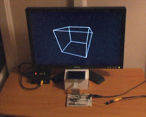
The TV contains a 75Ω resistor to ground on its composite video input. Two resistors are used on two PIC pins to form a voltage divider to produce the required output voltages (0V for sync, 0.3V for black and 1V for white). When the TV is disconnected the output of the circuit is 3.3V (the supply voltage, equivalent to a logic "high") as there's no load resistance to pull it to the correct 0.3V (a logic "low"). This can be used to periodically check whether a TV is connected and to switch between the LCD and TV output modes.
The above is rather vague, and I would recommend Rickard Gunée's article entitled How to generate video signals in software using PIC for more detailed information! The code for the demo can be downloaded from my website for those who are interested.
Update: I've updated my code to use the SPI peripheral in slave mode and use a timer and output compare unit to generate the clock signal. This regular clock signal produces pixels of identical sizes the new code can be downloaded here.
Booting CP/M 3 from an SD card
Wednesday, 23rd June 2010
Up to this point I have been running CP/M 2.2 on the Z80 computer. CP/M 3 adds a number of useful features, including the following:
- Support for more than 64KB RAM via banked memory.
- Standardised access to real-time clock for file date and time stamping.
- Improved text entry on the command-line when using the memory-banked version, such as the ability to move the cursor when editing and recall the previously entered line.
- Support for disks with physical sectors larger than the default record size of 128 bytes.
Switching to a banked memory system would require some new hardware in the form of a memory management unit so I have stuck with the simpler non-banked system for the time being. Support for physical disk sectors larger than 128 bytes is more interesting (SD cards use 512 byte "blocks") and real-time clocks are always useful so I have started working on updating to CP/M 3.
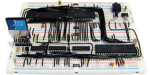
Z80 computer with new SD card slot (bottom left) and real-time clock (top right)
CP/M consists of three main pieces of software:
- A BIOS which exposes a small number of routines to perform primitive, hardware-specific operations (e.g. output a character to the console, read a raw sector from a disk, check if a key has been pressed).
- The BDOS which provides the main API for transient programs (e.g. read a complete line of input from the console, create a file, read a record from a file).
- The CCP, or console command processor, which provides the main user interface for loading and running other programs or performing some basic tasks via its built-in commands. This would be analogous to COMMAND.COM on DOS.
When working with CP/M 2.2 I had source files for these three pieces of software, so I just needed to implement the 17 BIOS functions, reassemble the three files to fixed addresses in memory and load them to these fixed addresses using the AVR when booting the computer. These three files were stored in the lower 8KB of the flash memory chip and were not accessible from within CP/M itself.
CP/M 3 proved to be a bit more of a challenge, as it is loaded slightly differently. The CCP is stored as a regular file named CCP.COM on the floppy disk you're booting from, so only the BIOS and BDOS need to be loaded from their hiding place at the start of the boot disk. These two pieces of software are merged into a single file named CPM3.SYS by a CP/M utility named GENCPM. To get this utility to work I needed to provide GENCPM with a hardware-specific BIOS3.SPR file that implemented the 31 BIOS routines. Fortunately, a file named BIOSKRNL.ASM is provided that implements most of the boilerplate code involved with writing a BIOS (you still have to provide the hardware-specific routines yourself, but your task is made much easier by following the template) so I just needed to recompile that for a non-banked system and link it with my handful of hardware-specific routines.
Ideally, CPM3.SYS would be stored on the regular file system with CCP.COM and the hidden boot loader would load CPM3.SYS for you. CP/M 3 does provide a small boot loader for this purpose (aptly named CPMLDR) which employs a cut-down BDOS and BIOS to load CPM3.SYS from the file system into memory for you. I haven't been able to get it to work, though, so I currently parse and load CPM3.SYS using some C code on the AVR. This works well enough for the time being, as can be seen in the above output generated by the computer when testing the real-time clock.
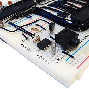
The time and date is maintained by a DS1307, an inexpensive eight-pin real-time clock and calendar chip that is shown in the middle of the above photograph. It is accessed over the I2C bus using a protocol that is natively supported by the AVR hardware. It uses binary-coded decimal to represent dates and times, which corresponds nicely to the time format used by CP/M; however, CP/M represents dates as a 16-bit integer counting the number of days since the 31st December 1977. I have used the algorithms on this website to convert dates to and from this format and the individual components.
The only downside of the DS1307 is that it only stores a two-digit year number, not the four digits one would hope for. This means that the century is discarded when setting the real-time clock, allowing for you to set a date that is then retrieved differently (truncated to the range 1930..2029). I haven't thought of a suitable solution to this problem just yet. I could use the AVR to act as the real-time clock, but I would then lose the advantage of the DS1307's battery backup that kicks in when the main power supply is removed.
The state of the DS1307 is effectively random at power-up. One of the first things the computer does when booting is to read the current date and time and check that all fields are within range. If not it resets them to midnight on the 1st January 1978 and displays a message to indicate that it has done so.
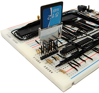
The SD card has been a bit of a headache to get working and though it currently only supports reading, not writing, it should hopefully be a useful addition to the computer. Rather than the previous arrangement of series rectifier diodes to drop the supply voltage and zener diodes to protect the inputs I'm using a dedicated 3.3V regulator to power the card and resistor voltage dividers to drop the 5V logic signals to around 3V (the closest I could get to 3.3V with the resistors I had to hand). I'm using the disk image from the old 512KB flash chip and treating the card as having 128 byte sectors so the arrangement is no more capable than before and in some cases quite a lot slower (reading a 128 byte record now entails reading a whole 512 byte block from the card then returning the desired 128 byte range within that block) but it seems to be as reliable as it used to be at least. SD cards append a CRC16 checksum when transferring data blocks so I can hopefully detect errors more easily and their on-board flash memory controller should perform wear-levelling, prolonging the life of the card.
To write the disk image to the card I used HxD which makes the job as easy as copy and paste. One problem I did have is that it displayed an "Access denied" error when attempting to write data, which I assume to be because something in Windows was using the card at the same time as HxD. I knocked together a short program for the AVR that wrote junk to the first block of the card, the result being that Windows no longer recognised the card's file system and HxD managed to write the data to the disk with no further problems.
Sockets for regular SD cards seem to be relatively expensive for what they are, but the above SD card reader cost a pound (what else?) from Poundland. A bit of work with a soldering iron and some desoldering tools yielded some useful components:
The crystal is unmarked and I'm hardly short of LEDs but the USB A connector could be a good way to reduce the size of a project that plugs into a USB port (USB B connectors are rather bulky) and the SD card slot works brilliantly for my needs here. There are cheaper and nastier ways to add an SD card slot to your project, but something like this feels more robust and has the advantage of reporting the state of the card's write protection switch.
Keyboard input and RAM disks make CP/M more useful
Wednesday, 16th June 2010
The hardware for the computer has changed in (mostly) subtle ways since the last post, with the exception of a PS/2 socket for connection to a keyboard.

PS/2 keyboards (which use the same protocol as the older AT keyboard) communicate with the host by clocking data in either direction (keyboard to host or host to keyboard) over two wires, appropriately named "clock" and "data". An AVR pin change interrupt is used to detect a change in state of the clock line and either input or output a bit on the data line depending on the current direction of data transmission. Incoming bytes generally relate to the scancode of the key that has just been pressed or released. These scancodes are looked up on a series of hard-coded tables to translate them into their corresponding ASCII characters. CP/M accesses the keyboard via two BIOS routines: CONST (2), which checks whether a character is available or not, and CONIN (3), which retrieves the character. I initially implemented these by simply reading from I/O port 2 (CONST) or port 3 (CONIN).
As keyboard input is polled, CP/M was wasting a lot of time reading from the AVR. Due to the AVR's relatively slow way to respond to I/O requests this was slowing down any program that needed to periodically call CONST (for example, BBC BASIC constantly checks for the Escape key when interpreting BASIC programs). I converted this polling system into an event driven one by connecting the AVR to the Z80's maskable interrupt pin, /INT. When a new key is received by the AVR it pulls /INT low to assert it. The Z80 responds to the interrupt request by setting an internal flag to remember that a key has been pressed and acknowledges the interrupt by outputting a value to port $38 (the Z80's maskable interrupt handler resides at a fixed address of $38 in memory, so this seemed like a sensible choice). The AVR detects this write to port $38 and returns /INT to its high state. The CONST routine can now directly return the value of this flag when polled (rather than having to request the flag from the AVR) which noticeably speeds up running programs. The flag is cleared when a key is read by calling CONIN.
I did have some difficulty getting the interrupt system to work; the Z80 has a number of different ways of responding to interrupts, two of which rely on fetching a value from the data bus by asserting /IORQ before an interrupt is serviced. IM 0 fetches an instruction from the bus and executes it, and IM 2 fetches the least significant byte of the address of the interrupt service routine to combine with the most significant byte stored in the I register. IM 1 (which is what I'm using) just jumps to the fixed address $38. However, I hadn't taken this additional data read into account and when the Z80 attempted to read from an I/O device the AVR was either putting nonsense on the bus or (deliberately) locking up with a message to indicate an unsupported operation. Fortunately you can easily tell the difference between a regular I/O request and an interrupt data request by checking the Z80's /M1 output pin, so with that addition things started working a bit more smoothly!
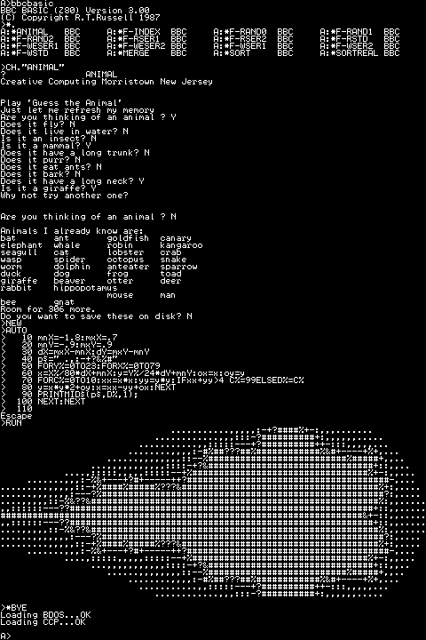
I'm still using terminal emulation software on my PC to view the output of the computer, though as I now have keyboard entry the results are a little more impressive than the few boot report lines and a prompt that were in the last entry. I still haven't worked out why my PC switches off or blue-screens when programming AVRs over the serial port, so I've soldered together a parallel port programmer for the time being.
The pinout of the programmer matches that of the website where I found the SI Prog design. The ATmega644P's SPI, power and reset pins that the programmer interfaces with are all adjacent, but not in the same order as the ones in the SI Prog, hence the small board to the right of the above photo which swaps the pin order around using wires soldered to its reverse (this saves a lot of breadboard space). The board in the middle plugs directly into the parallel port programmer and is used to program the 512KB flash memory chip I'm using for storage.
I haven't got around to implementing writing to this flash memory yet, unfortunately, though I have implemented a simple way to test a writable disk drive. The RAM chip I am using is a 128KB one, as Farnell didn't sell 64KB ones. The Z80 can only address 64KB without additional memory banking hardware, so I'd simply tied A16 low and was ignoring half of the memory. I have now edited the BIOS to expose two disk drives; the default A: (512KB of flash memory) and now B:, a 64KB RAM drive. A16 is now driven by the AVR; during normal operation, it is held low (giving the Z80 access to its usual 64KB) but during disk operations it can be driven high to grant the AVR access to the previously hidden storage.
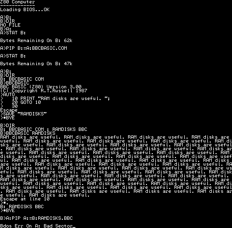
In the above test I use the STAT command to check free space, the PIP command to copy BBCBASIC.COM from A: (flash) to B: (RAM) then run BBC BASIC from the RAM disk, save a program then run it again by passing its filename as a command-line argument to BBC BASIC. At the end I try to copy the new program back to A:, but as there is no writing support for flash it keels over with a fairly unhelpful generic CP/M error.
Now that I've finally got something working in a vaguely usable manner, I hope I can start to research ways to make it better. Sorting out writing to flash would be a good start (I'm sorely tempted by jbb's suggestion to use an EEPROM to map logical floppy sectors to physical flash sectors) and I certainly hope to dig out my 320×240 pixel graphical LCD and driver for output instead of relying on a desktop PC. I'd also like to upgrade to CP/M 3 (I'm currently using CP/M 2.2) but when I last looked at that it seemed like a much more involved process so I decided to keep it simple. There's a fair mountain of stuff I need to take in, but I'm certainly learning a lot as I go (I only just realised tonight that CP/M was capable of graphics output, for one). I'd be a very happy chap if I could eventually run WordStar on this computer!
Combining a Z80 and an ATmega644P to boot CP/M
Monday, 14th June 2010
I've been working on a new Z80 computer over the last few days. I would say that I had been working on the existing Z80 computer were it not for the fact that this a completely new design.
The previous computer had two 32KB RAM chips to provide a total of 64KB RAM. To run a user program you need to get it into RAM somehow, so I also included a 128KB ROM chip which occupied the lower 16KB of the Z80's address space to provide the fixed operating system that could be used to load programs. By adding memory banking hardware I could select one of eight 16KB pages of ROM. The next 16KB was one of two banks of RAM from one RAM chip, and the final 32KB was mapped directly to the other RAM chip.
This is all fairly complicated, and not very flexible. Programs written for CP/M tend to be loaded into memory starting at address $0100, which is impossible with my old design as that section of memory is taken up by ROM.
Giving another device access to the buses
The Z80 accesses memory and other hardware devices using three buses; an eight-bit data bus which shuttles bytes of data between the various chips, a sixteen-bit address bus which addresses a location in memory or a particular I/O device, and a control bus which contains numerous lines that specify the type of operation (for example, if /MREQ and /WR go low together it indicates that a byte is being written to memory, or if /IORQ and /RD go low together it indicates that a byte is being read from an I/O device).
There is also a pin named /BUSREQ that can be used to request access to these buses. The Z80 will periodically check this pin and if it is held low it will put the data, address and control buses into a high-impedance state and drive /BUSACK low to acknowledge this. This effectively removes the Z80 from the circuit, and another device can now drive the buses.
;if(img.style.backgroundImage){img.style.backgroundImage='url('+img.src+')';img.src=imgs[img.src.indexOf(imgs[1])<0?1:2]}else{img.style.backgroundImage='url('+img.src+')';img.src=imgs[2];};void(0);)
This is the feature which I have based the new design around — the current prototype is pictured above. It features a Z80 and 128KB of SRAM (only 64KB is currently addressable) on the upper board. On the lower board is an ATmega644P microcontroller, which is used to start the computer.
When the circuit is reset, the ATmega644P requests access to the buses from the Z80. When access has been granted, it proceeds to copy the CP/M BIOS from the 512KB flash memory IC to a specific location in RAM (currently $F200). It then writes the Z80 jump instruction jp $F200 to the start of memory, returns control of the buses to the Z80 and pulses its /RESET pin. The CP/M BIOS then runs directly on the Z80.
As the ATmega644P doesn't have enough pins to drive all of the buses directly, I've added sixteen GPIO pins by using two MCP23S08 8-bit I/O expander chips. These are used to drive or sample the Z80 address bus; the data and control buses are driven or sampled directly by the GPIO ports on the ATmega644P.
Using a slow to respond microcontroller for I/O
The Z80 is most useful if it can talk to the outside world somehow, which is usually achieved by reading from or writing to I/O devices. In my previous design I built these out of latches and lots of glue logic. As I've added a powerful microcontroller to the computer which features a number of useful on-board peripherals, it would seem sensible to use that instead.
One problem with this idea is that the Z80 expects to read or write to an I/O device in a mere four clock cycles. The AVR has a delay between an interrupt occurring (such as a pin state changing) and executing interrupt service routine of at least five clock cycles. Even though the AVR is running at twice the clock speed of the Z80 this still doesn't provide much time to sample the address bus and perform some useful action before returning a value to the Z80. Fortunately, the Z80 has another useful pin, /WAIT, specifically to address this concern. By pulling this pin low the Z80 can be stalled, allowing the I/O device plenty of time to respond. I have included a 7474 D-type flip-flop as an SR latch to control the /WAIT pin. When the Z80's /IORQ pin goes low the flip-flop is reset, which pulls the /WAIT pin low. When the AVR notices that the /IORQ line has gone low it samples the address bus, performs the requisite task then sets the flip-flop, which drives the /WAIT pin high again and the Z80 continues executing the program.
The 7474 is a dual D-type flip-flop, so I have used the second flip-flop to halve the AVR's 20MHz clock signal to provide the 10MHz clock for the Z80.
CP/M interacts with the host computer by calling numbered BIOS functions. I have implemented a number of these BIOS functions by outputting a value to a port number that matches the BIOS function number. For example, CONOUT is function number four and is used to send the character in register C to the console.
CONOUT:
    ld a,c
    out (4),a
    ret
The AVR detects a write to port 4 and sends the incoming byte to one of its UARTs. I have connected this UART to a simple transistor inverter (pictured in the top right of the above photograph) and plugged the output from that into one of my PC's serial ports, so by running a terminal emulator I can see the output of CP/M on the screen. I have implemented only a handful of other functions (WBOOT outputs a value to port 1 to indicate that I should load the BDOS and CCP into RAM from the flash memory and READ can be used to copy 128 byte floppy disk sectors from flash memory to Z80 RAM) so the results are not exactly impressive:
Loading BIOS...OK
Loading BDOS...OK
Loading CCP...OK

A>
As I haven't implemented console input yet there's no way to type at the prompt, but that it gets that far is encouraging.
I haven't implemented writing to the flash memory due to a mistake I made when reading its datasheet. When writing to flash memory the value you write is ANDed with the data that's already there (you can only set a 1 bit to a 0 bit, but not vice-versa) – this is referred to as programming. If you want to write a 1 bit you have to erase the memory before writing to it (this is unsurprisingly referred to as erasing). Flash memory can be split into pages (small regions, in this case 256 bytes) and sectors (large regions, in this case 64KB). You can often program any number of bytes (up to a page at a time, aligned to page boundaries) but can only erase in larger blocks — pages, sectors, or the entire memory (bulk erase). I thought that the flash memory ICs I bought supported page erasing, but they only support sector erasing. CP/M transfers data between floppy disks and RAM in 128 byte floppy disk sectors, so to write an updated sector I would need to read 64KB from the flash memory, update a 128 byte region within it, erase an entire flash sector, then program the 64KB back to it. This would be very slow and quickly wear out the flash memory, so I am looking for some replacement flash memory ICs which do support page erase.
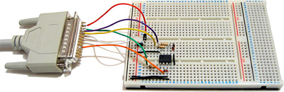
To copy the system files and a sample disk image to the flash memory I cobbled together the above parallel port programmer which is driven by an application cobbled together in C#. It's rather slow but gets the job done — unlike my AVR programmer. After finally managing to get CP/M to boot in a satisfactory manner I made a few tweaks to the AVR program and hit the "Build and Program" button in the editor. The code built, but rather than program the AVR my computer switched off. No error message, not even a blue screen, just a sudden and surprising power down. Since then I've only managed to talk to the AVR once; every other time has resulted in either a power down or blue screen. I had hoped to add some keyboard handling routines to the project to at least be able to interact with CP/M, but after fiddling around for an hour and a half without managing to get anything working again I gave up. I wish I knew why it suddenly stopped working, after hours of reliable service — maybe it's a hint that it's time to buy a proper USB debugger rather than the cheap and cheerful home-made serial port programmer I've been using!
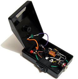
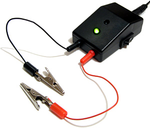
One equally cheap but useful addition to my tools is the above 5V power supply (yes, it's just a 7805 regulator in a box). Every project I have built needs a 5V supply from somewhere, which usually comes from a 7.5V wall wart power supply unit regulated to 5V with a 7805. This takes up valuable breadboard space and the weight of the cable from the power supply tends to drag the breadboard around the smooth surface of my desk, so having a dedicated box with an on-off switch, indicator LED, reverse voltage protection and an easy way to connect to the circuit via 2mm sockets is very handy indeed.
I now need to find a way to program AVRs without my PC switching itself off before I can make any more progress on the project...
USB remote control receiver for PowerDVD
Monday, 7th June 2010
I enjoy watching films and mainly do so sitting at my desktop PC. This has taught me that cheap office chairs are not the most comfortable things to sit on for extended periods of time, especially when the next room contains a comfortable bean bag and a good place to stick a screen. A gap between the two rooms allows me to pass cables from one to the other, and after purchasing a 10m DVI-D cable and a USB extension lead on eBay I had both picture and sound sorted out (I use a USB sound "card"). This left me with one final problem: how to control the PC through a wall.
One possibility would be to extend the lead on my keyboard, but its media buttons light up (bothersome in a darkened room) and some of the keyboard shortcuts in PowerDVD (such as Ctrl+P for the popup menu when watching Blu-ray discs) are tricky to hit in the dark. Given my fondness for infra-red remote controls building a remote control receiver would seem like both an interesting and useful way to spend a weekend.
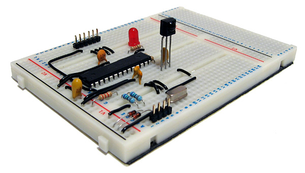
Rather than build something that relied on some Windows software to translate received remote control signals into keystrokes I decided to use the free V-USB library to construct something that showed up in Windows as a standard USB keyboard. One of the sample V-USB projects is a USB keyboard, which made getting started much easier! The above photograph shows the initial prototype, based around an ATmega168. The tall three-legged component sticking up out of the board is a TSOP2438, which is an infra-red receiver and demodulator. This is tuned to the 38kHz carrier employed by most remote controls and outputs a logic low or logic high depending on the presence or absence of such a signal. The ATmega168 is programmed to time the incoming signal and passes this timing information to a collection of routines that attempt to decode it. I have currently two decoders, one for the NEC protocol and another for SIRCS — information about some common protocols can be found on this website.
The choice of these two protocols is down to the remote controls I have around me. The one that offered me the most useful buttons was the PlayStation 2 DVD remote control (SIRCS), though this is missing some useful controls, such as volume and the red, green, yellow and blue buttons. To remedy this I went and bought a cheap universal remote control from Clas Ohlson. After hunting through several of the modes I settled on the Clas Ohlson DVD one (0815) as most of the buttons work in this mode (the only unshifted one that doesn't is the record button, and I can live without it). In this mode the remote control uses the NEC protocol.
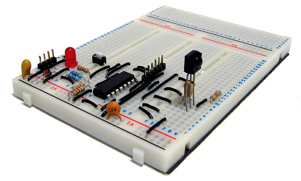
To turn the receiver into something more conveniently sized I decided to switch from the 28-pin ATmega168 to the 14-pin ATtiny84, shown in the above photograph. The compiled program was already small enough to fit into the reduced memory, and the only modification I had to make was to amend two timing routines to share the same timer peripheral as the ATtiny84 only has two timers, not the three I'd been using on the ATmega168.
I also opted to add a switch to the design. One problem with supporting both Blu-ray and DVD is that the way you navigate menus is quite different between the two; Blu-ray discs use a simple popup menu (Ctrl+P) which appears on top of the film, whereas DVDs seem to offer a number of different menu commands — the two most common ones being "Title menu" (no shortcut) and "Root menu" (J). PowerDVD also lets you choose from a list of DVD menus in a context menu with one shortcut (L). I set the button on the receiver to switch between "Blu-ray" and "DVD" modes; in Blu-ray mode, the menu button sends Ctrl+P and in DVD mode the menu button sends L.
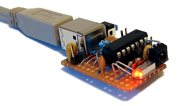
I bought an enclosure that is, in retrospect, a little too small. The above photograph shows the receiver assembled on stripboard with a fairly cramped layout. Fortunately there was sufficient room to include pin headers on the board, which will allow me to plug in a programmer to modify the software should I need to in the future. The LED on the front serves as simple user feedback — it flashes whenever it receives a valid command and sends a keystroke back to the PC. When the mode is toggled between Blu-ray and DVD menus it flashes to indicate the new mode — a long flash followed by a single short one for Blu-ray, a long flash followed by two short ones for DVD.
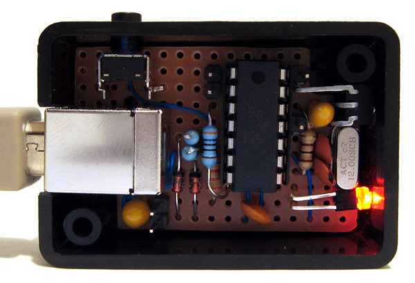
Overall, I'm quite happy with the way it turned out. It works well enough for my needs, though as those needs only extend as far as PowerDVD and a particular remote control it's rather basic and much more could be done with the hardware. I have uploaded the source code and a schematic for the project to my website as it currently stands for those who are interested.
Superprobe
Saturday, 10th April 2010
I have recently been working on building my own Superprobe. This is a cheap and simple tool based around a single PIC 16F870, a four-digit display and a handful of other parts. Hardware details and software can be found on the Superprobe section of the Mondo Technology website.
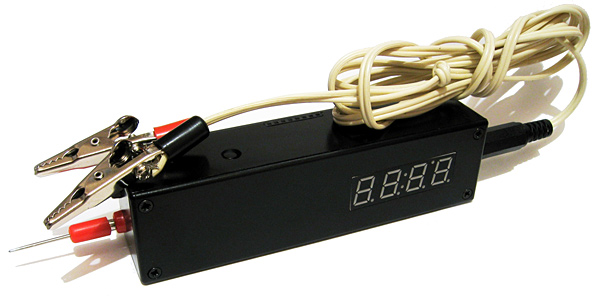
As the name suggests, at its simplest the Superprobe can be used as a logic probe, displaying an L, H or - if it touches a point in the circuit that is in a low, high or floating state. What makes it so "super" is that by using the two input buttons you can switch it to a different mode. The supplied software provides seventeen different modes, including a logic pulser, frequency counter, voltmeter, capacitance meter, signal generator and serial ASCII data output.
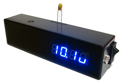
Measuring a 10µF capacitor.
Having such a wide range of functions for such a modest part count made this a very attractive project to build. Unfortunately, I couldn't find a 16F870 so used the pin-compatible 16F876A instead; porting the code from the older microcontroller mainly involved changing the list p=16f870 directive. I did notice that the probe didn't seem to save its settings when powering down as it should, so I copied the EEPROM reading and writing code from the 16F876A datasheet into the source to replace the existing code which seemed to fix it.
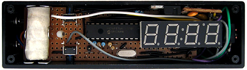
The insides of the Superprobe.
As I couldn't find a suitable low drop-out 5V regulator I opted to use a conventional L7805 regulator. This means that the input voltage has to be at least two volts higher than the output; I normally power circuits from a 7.5V or 9V supply anyway so this isn't too much of a problem. Finding a suitable battery to go inside the case was more of a challenge; there's insufficient room for the typical 9V PP3, sadly. A bit of hunting for "7.5V battery" led me to a suitable battery with a variety of names and a rather high price. Aided by a ruler and the dimensions on the above website it seems that the A175 is exactly the same size as five LR44/AG13 cells stacked on top of eachother (coincidence? I think not). A reputable high street shop noted for the quality of its goods sold a card of forty button cells (including ten AG13 cells), so five of those and a bit of masking tape provided me with a passable imitation. Sparing no expense, the battery holder is constructed from paper clips.
The 16F876A has more program space and SRAM than the 16F870, making developing software in C more viable. Not all of of the original software's features were especially useful to me, and I was likely to want to add new modes myself in the future, so set about reimplementing the functions that I did find handy in C. The result is quite a bit easier to modify; for example, the above photograph demonstrating the measurement of a capacitor shows a value with an SI prefix (10.1u for a 10µF capacitor). All one needs to do to display such a number on the display is call display_print_float(10.1e-6f); – the code does the rest for you. Sadly, this does inflate the size of the code significantly and my current version of the code only squeezes 11 functions into a much larger chip (compared to the 17 on the original).
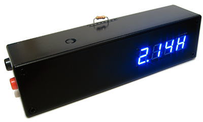
Measuring a 2.2KΩ resistor.
One of the new modes is a resistance meter. This works by pulling the probe tip high using a known resistance (5KΩ, 10KΩ or 100KΩ) and combining this with the resistor to be measured between the probe tip and ground to form a voltage divider. The output of the voltage divider is measured, and from that the resistance of the resistor being tested can be determined. The ability to use multiplication, division and floating point arithmetic makes this easy to program in C; much more so than it would have been in assembly, at least!
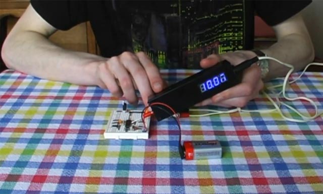
I have recorded a video demonstrating the Superprobe. The code for my variation on the theme can be downloaded here, and can be compiled with the free ("lite") edition of the HI-TECH C compiler.
Controlling a PG320240H-P9 with a dsPIC33FJ128GP802
Sunday, 21st March 2010
In a previous entry I mentioned that I had purchased a PG320240H-P9 graphical LCD. This is a 320×240 white-on-blue pixel display, and it does not have an on-board controller or RAM. To display something on it you need to constantly refresh it with picture data; in this instance, sending four pixels at a time, starting from the top left and working from left to right, top to bottom — a bit like the scanning pattern of a CRT monitor.
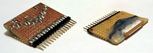
Connecting a circuit to the LCD is made slightly more tricky by its use of a 16-pin 1mm flexible flat cable. To get around this I soldered together an adaptor using a suitable FCC connector, pin strip, piece of stripboard and a fairly excessive quantity of hot melt adhesive. Even more tricky was the lack of a suitable datasheet for the LCD. After some digging I located this one for the PG320240WRM-HNNIS1 — it's slightly different, but contains timing diagrams and specifications that seem to work with the LCD I bought. One thing I still haven't worked out is the contrast adjustment; a 5K variable resistor between 0V and the relevant pin seems to have had the best results thus far. A helpful webpage, Graphical LCD controller for ST8024+ST8016 based displays, has a plain English description of how to drive the LCD, though as far as I'm aware the M pin should have its logic level toggled every frame, giving you a "glass" frequency of half of the refresh rate, not 200Hz-400Hz. The lack of a proper datasheet makes these things a little complicated!
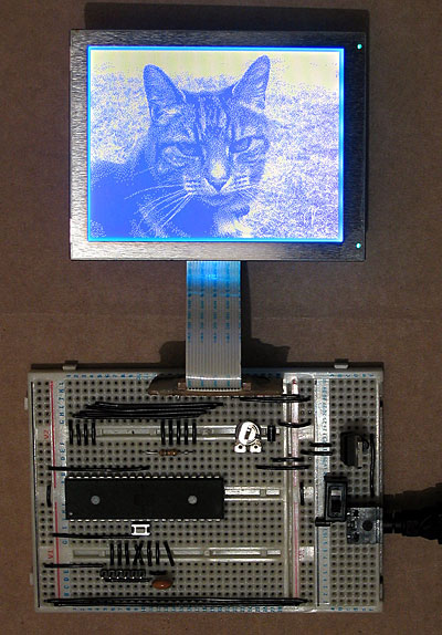
My first attempt to drive the LCD involved an ATmega644P, a microcontroller with 64KB of flash ROM and 4KB of RAM. The above photo shows it displaying a picture of a cat, which was stored in ROM and output using the following code:
#include <stdint.h>
#include <avr/io.h>
#include <avr/pgmspace.h>

#define LCD_FLM   (6)
#define LCD_M     (5)
#define LCD_C1    (4)
#define LCD_C2    (3)
#define LCD_D_OFF (2)

#define LCD_CONTROL_PORT (PORTC)
#define LCD_CONTROL_PIN  (PINC)
#define LCD_CONTROL_DDR  (DDRC)

#define LCD_DATA_PORT    (PORTA)
#define LCD_DATA_PIN     (PINA)
#define LCD_DATA_DDR     (DDRA)

#include "cat.h"

int main(void) {

    // Make control pins outputs.
    LCD_CONTROL_DDR |= _BV(LCD_FLM) | _BV(LCD_M) | _BV(LCD_C1) | _BV(LCD_C2) | _BV(LCD_D_OFF);

    // Make data pins outputs.
    LCD_DATA_DDR |= 0b1111;

    // Enable the LCD.
    LCD_CONTROL_PORT |= _BV(LCD_D_OFF);

    for(;;) {

        // Toggle the M pin to provide the LCD AC voltage.
        LCD_CONTROL_PIN |= _BV(LCD_M);

        const uint8_t* picture_ptr = cat_picture;

        // Scan 240 rows in the image.
        for (uint8_t row = 0; row < 240; ++row) {

            // Begin the line.
            LCD_CONTROL_PIN |= _BV(LCD_C1);
            LCD_CONTROL_PIN |= _BV(LCD_C1);

            if (row < 2) LCD_CONTROL_PIN |= _BV(LCD_FLM);

            // Send 40 eight-bit words.
            for (uint8_t column = 0; column < 40; ++column) {
                LCD_DATA_PORT = pgm_read_byte(picture_ptr) >> 4;
                LCD_CONTROL_PIN |= _BV(LCD_C2);
                LCD_CONTROL_PIN |= _BV(LCD_C2);
                LCD_DATA_PORT = pgm_read_byte(picture_ptr);
                LCD_CONTROL_PIN |= _BV(LCD_C2);
                LCD_CONTROL_PIN |= _BV(LCD_C2);
                ++picture_ptr;
            }
        }
    }

}
A 320×240 display has 76,800 pixels, and if you store each pixel as a single bit (so eight pixels per byte) you need 9600 bytes to store a complete frame, which clearly won't fit in the 4KB offered by the ATmega644P. Rather than upgrade to an AVR with more memory, I jumped to the dsPIC33FJ128GP802, a 16-bit microcontroller with 16KB of RAM. As well as quadrupling the RAM from the ATmega644P it also doubles the program memory (128KB from 64KB) and speed (40 MIPS from 20 MIPS). When working with AVRs I'd been using a slow home-made serial programmer, and rather than continue with this sorry state of affairs (lack of debugging capabilities is never fun, especially when it takes over a minute to program the microcontroller) I treated myself to a PICkit 3 Debug Express.
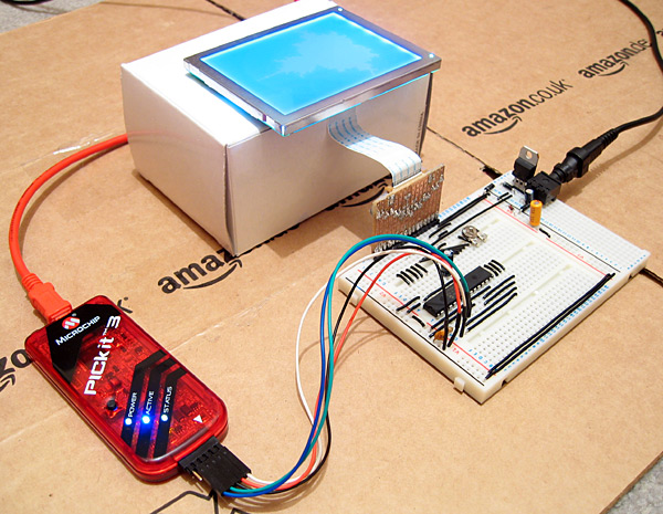
The above photo shows the LCD connected to the microcontroller as well as the PICkit 3. The dsPIC33FJ128GP802 requires a voltage supply from 3.0V to 3.6V, not the 5V I am used to, so to power it I have put two IN4001 rectifier diodes in series with the 5V regulator output. Each diode incurs a voltage drop of 0.7V, producing 3.6V for the rest of the circuit. The LCD is powered from the main 5V supply, but it seems happy with the 3.6V logic "high" from the dsPIC.
The LCD is connected to the dsPIC as follows:
- FLM to RB15
- M to RB14
- C1 to RB13
- C2 to RB12
- /D_OFF to RB11
- D0~D3 to RA0~RA3
A 10K resistor is included between /D_OFF and ground. This is very important, as it holds the /D_OFF line low when RB11 is floating (e.g. during reset), forcing the display off — if the display is powered, but is not being actively refreshed, the LCD panel can become overloaded and damaged.
I have knocked together a simple demo that shows a few different graphics on the LCD. The LCD is constantly refreshed by an interrupt service routine that runs in the background, leaving some CPU time to the user program. As there is only enough RAM for a single frame buffer, animation has to be quite simple to avoid flickering, but I've still managed to include my favourite spinning cube.
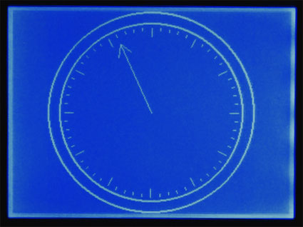
The project can be downloaded here. I'm still getting to grips with the dsPIC series; the code is likely to be pretty awful, and I still have a problem where the dsPIC resets itself every couple of minutes (I'm not really sure if this is a software or hardware issue). Still, it's a start, and I hope that I can use this LCD as the display for my Z80 computer project.
Update: Having seen this post, the chap who originally suggested that I investigate the dsPIC33FJ128GP802 sent me an email with some advice, chiefly about my poor power supply, missing decoupling capacitors and use of an electrolytic capacitor on the VCAP pin. I have since replaced the two rectifier diode affair with a proper 3.3V regulator for the power supply, added a decoupling capacitor across AVDD/AVSS and moved the decoupling capacitor between VDD/VSS closer to the microcontroller. I have also ordered some tantalum capacitors to replace the electrolytic one. A bit of debugging found that the watchdog timer is responsible for the spurious resets; I have disabled it in the code for the time being, which has stopped the resets.
ATmega644P CHIP-8/SCHIP interpreter
Sunday, 7th March 2010
In an attempt to solve the screen resolution problem issue I've bought a very cheap 320×240 pixel graphical LCD – a PG320240H-P9 on eBay for $24. Part of the reason for its cheapness may be down to its the lack of a controller; you need to constantly refresh the LCD with pixel data yourself (easier to use modules have integrated controllers that refresh the display for you from some on-board RAM). If I manage to get it working I'll have a 128×64 pixel graphical LCD going spare – finding a use for it could make an interesting project.
I have a bit of a soft spot for the CHIP-8 programming language, having previously written an few implementations. The CHIP-8 environment requires just under 3.5KB of RAM, and my recent investment in an ATmega644P boasting 4KB of RAM provided me with a microcontroller that was up to the task.
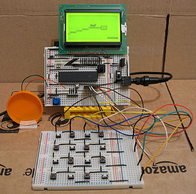
Beyond the ATmega644P and LCD the hardware is pretty simple; a potentiometer is provided to adjust the speed of the interpreter when it's running, from 1/8th speed up to 8× speed. Sound is output using a piezo transducer, which I've taped to the hard plastic lid from a tube of chocolates to amplify it. Games rely on a 4×4 hex keypad for input, and as I do not have a 4×4 keypad – hex or otherwise – I assembled my own on another breadboard. I don't even have sixteen switches of the same type, hence the mixture in the above photo. A schematic of the hardware can be downloaded in PDF format.
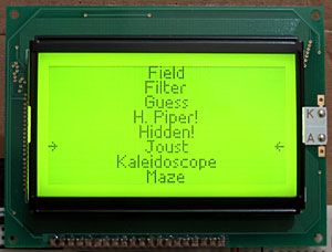
When you reset the circuit a list of all of the programs stored on the microcontroller is shown on the LCD. The 64KB of flash memory on the ATmega644P is enough to store the code for the interpreter and all of the CHIP-8 and SCHIP games available on the Internet. For a change I've decided to have a go at designing a variable width font rather than use one of my existing fixed-width fonts; I don't think it looks too shabby.
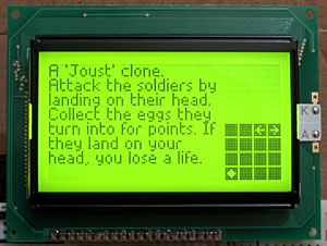
When a game has been selected a (gramatically incorrect) summary of the game is shown. To the right of the screen is a 4×4 grid informing the player which key does what; arrows for directional controls, a diamond for "fire" or confirmation actions and a tick/cross for yes/no input. There doesn't seem to be any particular convention for keypad input in CHIP-8/SCHIP games, which makes this feature invaluable!
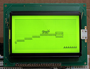
Thinking about CP/M
Wednesday, 24th February 2010
It's been some time since I worked on my Z80 computer project, but the recent electronics projects I've completed have got me thinking about it again.
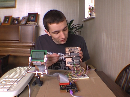
I did record a video to demonstrate the basic parts of the computer and some of its flaws a few months ago, which can be seen above. However, I'm now thinking of a more radical redesign than fixing the I/O board's shortcomings.
One of the reasons for my lack of motivation is that even if I did get something working I wouldn't have much software to run on it; it would be a lot of work to write software that only ran on that one particular machine. BBC BASIC helps somewhat, but an even better solution would be to model the device on an existing machine and run its operating system on it.
Fortunately, there was a popular operating system for the 8080 (and, by extension, the Z80) – CP/M. This is a very simple operating system that inspired DOS. Crucially, it is not hardware-specific, the source code is available and there is a wide range of software available for it, including BBC BASIC.
CP/M is made up of three main components. At the highest level is the Console Command Processor, or CCP. This provides the command-line interface, a handful of built-in commands and handles loading and executing external programs. It achieves this with the aid of the Basic Disk Operating System, or BDOS, which exposes a number of useful routines for a variety of tasks, such as outputting text to the display, searching for files on the disk or reading console input.
Both of the above components are machine-independent – they simply need to be copied to the correct address in RAM when the computer starts. Relocating them to a particular address requires setting a single value in their respective source files and reassembling them, which is nice and easy. It's the third component – the Basic I/O System, or BIOS – that requires a bit more work. This is the only part that is tailored to a particular machine's hardware, and my current implementation is listed below.
CCP    = $DC00
BDOS   = $E406
BIOS   = $F200

IOBYTE = $0003
CDISK  = $0004

DMAAD  = $0008
CTRACK = $000A
CSEC   = $000C

.org BIOS

	jp BOOT    ; COLD START
WBOOTE
	jp WBOOT   ; WARM START
	jp CONST   ; CONSOLE STATUS
	jp CONIN   ; CONSOLE CHARACTER IN
	jp CONOUT  ; CONSOLE CHARACTER OUT
	jp LIST    ; LIST CHARACTER OUT
	jp PUNCH   ; PUNCH CHARACTER OUT
	jp READER  ; READER CHARACTER OUT
	jp HOME    ; MOVE HEAD TO HOME POSITION
	jp SELDSK  ; SELECT DISK
	jp SETTRK  ; SET TRACK NUMBER
	jp SETSEC  ; SET SECTOR NUMBER
	jp SETDMA  ; SET DMA ADDRESS
	jp READ    ; READ DISK
	jp WRITE   ; WRITE DISK
	jp LISTST  ; RETURN LIST STATUS
	jp SECTRAN ; SECTOR TRANSLATE

DISKPARAM
	.dw $0000  ; No sector translation.
	.dw $0000  ; Scratch
	.dw $0000  ; Scratch
	.dw $0000  ; Scratch
	.dw DIRBUF ; Address of a 128-byte scratch pad area for directory operations within BDOS. All DPHs address the same scratch pad area.
	.dw DPBLK  ; Address of a disk parameter block for this drive. Drives with identical disk characteristics address the same disk parameter block.
	.dw CHK00  ; Address of a scratch pad area used for software check for changed disks. This address is different for each DPH.
	.dw ALL00  ; Address of a scratch pad area used by the BDOS to keep disk storage allocation information. This address is different for each DPH.

DIRBUF
	.fill 128

DPBLK           ; DISK PARAMETER BLOCK, COMMON TO ALL DISKS
	.DW 26      ; SECTORS PER TRACK
	.DB 3       ; BLOCK SHIFT FACTOR
	.DB 7       ; BLOCK MASK
	.DB 0       ; NULL MASK
	.DW 242     ; DISK SIZE-1
	.DW 63      ; DIRECTORY MAX
	.DB 192     ; ALLOC 0
	.DB 0       ; ALLOC 1
	.DW 16      ; CHECK SIZE
	.DW 2       ; TRACK OFFSET

CHK00
	.fill 16

ALL00
	.fill 31

; =========================================================================== ;
; BOOT                                                                        ;
; =========================================================================== ;
; The BOOT entry point gets control from the cold start loader and is         ;
; responsible for basic system initialization, including sending a sign-on    ;
; message, which can be omitted in the first version.                         ;
; If the IOBYTE function is implemented, it must be set at this point.        ;
; The various system parameters that are set by the WBOOT entry point must be ;
; initialized, and control is transferred to the CCP at 3400 + b for further  ;
; processing. Note that register C must be set to zero to select drive A.     ;
; =========================================================================== ;
BOOT
	xor a
	ld (IOBYTE),a
	ld (CDISK),a
	jp GOCPM

; =========================================================================== ;
; WBOOT                                                                       ;
; =========================================================================== ;
; The WBOOT entry point gets control when a warm start occurs.                ;
; A warm start is performed whenever a user program branches to location      ;
; 0000H, or when the CPU is reset from the front panel. The CP/M system must  ;
; be loaded from the first two tracks of drive A up to, but not including,    ;
; the BIOS, or CBIOS, if the user has completed the patch. System parameters  ;
; must be initialized as follows:                                             ;
;                                                                             ;
; location 0,1,2                                                              ;
;     Set to JMP WBOOT for warm starts (000H: JMP 4A03H + b)                  ;
;                                                                             ;
; location 3                                                                  ;
;     Set initial value of IOBYTE, if implemented in the CBIOS                ;
;                                                                             ;
; location 4                                                                  ;
;     High nibble = current user number, low nibble = current drive           ;
;                                                                             ;
; location 5,6,7                                                              ;
;     Set to JMP BDOS, which is the primary entry point to CP/M for transient ;
;     programs. (0005H: JMP 3C06H + b)                                        ;
;                                                                             ;
; Refer to Section 6.9 for complete details of page zero use. Upon completion ;
; of the initialization, the WBOOT program must branch to the CCP at 3400H+b  ;
; to restart the system.                                                      ;
; Upon entry to the CCP, register C is set to thedrive;to select after system ;
; initialization. The WBOOT routine should read location 4 in memory, verify  ;
; that is a legal drive, and pass it to the CCP in register C.                ;
; =========================================================================== ;
WBOOT

GOCPM
	ld a,$C3      ; C3 IS A JMP INSTRUCTION
	ld ($0000),a  ; FOR JMP TO WBOOT
	ld hl,WBOOTE  ; WBOOT ENTRY POINT
	ld ($0001),hl ; SET ADDRESS FIELD FOR JMP AT 0

	ld ($0005),a  ; FOR JMP TO BDOS
	ld hl,BDOS    ; BDOS ENTRY POINT
	ld ($0006),hl ; ADDRESS FIELD OF JUMP AT 5 TO BDOS

	ld bc,$0080   ; DEFAULT DMA ADDRESS IS 80H
	call SETDMA

	ei            ; ENABLE THE INTERRUPT SYSTEM
	ld a,(CDISK)  ; GET CURRENT DISK NUMBER
	ld c,a        ; SEND TO THE CCP
	jp CCP        ; GO TO CP/M FOR FURTHER PROCESSING

; =========================================================================== ;
; CONST                                                                       ;
; =========================================================================== ;
; You should sample the status of the currently assigned console device and   ;
; return 0FFH in register A if a character is ready to read and 00H in        ;
; register A if no console characters are ready.                              ;
; =========================================================================== ;
CONST
	out (2),a \ ret

; =========================================================================== ;
; CONIN                                                                       ;
; =========================================================================== ;
; The next console character is read into register A, and the parity bit is   ;
; set, high-order bit, to zero. If no console character is ready, wait until  ;
; a character is typed before returning.                                      ;
; =========================================================================== ;
CONIN
	out (3),a \ ret

; =========================================================================== ;
; CONOUT                                                                      ;
; =========================================================================== ;
; The character is sent from register C to the console output device.         ;
; The character is in ASCII, with high-order parity bit set to zero. You      ;
; might want to include a time-out on a line-feed or carriage return, if the  ;
; console device requires some time interval at the end of the line (such as  ;
; a TI Silent 700 terminal). You can filter out control characters that cause ;
; the console device to react in a strange way (CTRL-Z causes the Lear-       ;
; Siegler terminal to clear the screen, for example).                         ;
; =========================================================================== ;
CONOUT
	out (4),a \ ret

; =========================================================================== ;
; LIST                                                                        ;
; =========================================================================== ;
; The character is sent from register C to the currently assigned listing     ;
; device. The character is in ASCII with zero parity bit.                     ;
; =========================================================================== ;
LIST
	out (5),a \ ret

; =========================================================================== ;
; PUNCH                                                                       ;
; =========================================================================== ;
; The character is sent from register C to the currently assigned punch       ;
; device. The character is in ASCII with zero parity.                         ;
; =========================================================================== ;
PUNCH
	out (6),a \ ret

; =========================================================================== ;
; READER                                                                      ;
; =========================================================================== ;
; The next character is read from the currently assigned reader device into   ;
; register A with zero parity (high-order bit must be zero); an end-of-file   ;
; condition is reported by returning an ASCII CTRL-Z(1AH).                    ;
; =========================================================================== ;
READER
	out (7),a \ ret

; =========================================================================== ;
; HOME                                                                        ;
; =========================================================================== ;
; The disk head of the currently selected disk (initially disk A) is moved to ;
; the track 00 position. If the controller allows access to the track 0 flag  ;
; from the drive, the head is stepped until the track 0 flag is detected. If  ;
; the controller does not support this feature, the HOME call is translated   ;
; into a call to SETTRK with a parameter of 0.                                ;
; =========================================================================== ;
HOME
	ld bc,0
	jp SETTRK

; =========================================================================== ;
; SELDSK                                                                      ;
; =========================================================================== ;
; The disk drive given by register C is selected for further operations,      ;
; where register C contains 0 for drive A, 1 for drive B, and so on up to 15  ;
; for drive P (the standard CP/M distribution version supports four drives).  ;
; On each disk select, SELDSK must return in HL the base address of a 16-byte ;
; area, called the Disk Parameter Header, described in Section 6.10.          ;
; For standard floppy disk drives, the contents of the header and associated  ;
; tables do not change; thus, the program segment included in the sample      ;
; CBIOS performs this operation automatically.                                ;
;                                                                             ;
; If there is an attempt to select a nonexistent drive, SELDSK returns        ;
; HL = 0000H as an error indicator. Although SELDSK must return the header    ;
; address on each call, it is advisable to postpone the physical disk select  ;
; operation until an I/O function (seek, read, or write) is actually          ;
; performed, because disk selects often occur without ultimately performing   ;
; any disk I/O, and many controllers unload the head of the current disk      ;
; before selecting the new drive. This causes an excessive amount of noise    ;
; and disk wear. The least significant bit of register E is zero if this is   ;
; the first occurrence of the drive select since the last cold or warm start. ;
; =========================================================================== ;
SELDSK
	ld hl,DISKPARAM
	ld a,c
	or a
	ret z
	ld hl,$0000 ; Only disc 0 is supported.
	ret

; =========================================================================== ;
; SETTRK                                                                      ;
; =========================================================================== ;
; Register BC contains the track number for subsequent disk accesses on the   ;
; currently selected drive. The sector number in BC is the same as the number ;
; returned from the SECTRAN entry point. You can choose to seek the selected  ;
; track at this time or delay the seek until the next read or write actually  ;
; occurs. Register BC can take on values in the range 0-76 corresponding to   ;
; valid track numbers for standard floppy disk drives and 0-65535 for         ;
; nonstandard disk subsystems.                                                ;
; =========================================================================== ;
SETTRK
	ld (CTRACK),bc
	ret

; =========================================================================== ;
; SETSEC                                                                      ;
; =========================================================================== ;
; Register BC contains the sector number, 1 through 26, for subsequent disk   ;
; accesses on the currently selected drive. The sector number in BC is the    ;
; same as the number returned from the SECTRAN entry point. You can choose to ;
; send this information to the controller at this point or delay sector       ;
; selection until a read or write operation occurs.                           ;
; =========================================================================== ;
SETSEC
	ld (CSEC),bc
	ret

; =========================================================================== ;
; SETDMA                                                                      ;
; =========================================================================== ;
; Register BC contains the DMA (Disk Memory Access) address for subsequent    ;
; read or write operations. For example, if B = 00H and C = 80H when SETDMA   ;
; is called, all subsequent read operations read their data into 80H through  ;
; 0FFH and all subsequent write operations get their data from 80H through    ;
; 0FFH, until the next call to SETDMA occurs. The initial DMA address is      ;
; assumed to be 80H. The controller need not actually support Direct Memory   ;
; Access. If, for example, all data transfers are through I/O ports, the      ;
; CBIOS that is constructed uses the 128 byte area starting at the selected   ;
; DMA address for the memory buffer during the subsequent read or write       ;
; operations.                                                                 ;
; =========================================================================== ;
SETDMA
	ld (DMAAD),bc
	ret

; =========================================================================== ;
; READ                                                                        ;
; =========================================================================== ;
; Assuming the drive has been selected, the track has been set, and the DMA   ;
; address has been specified, the READ subroutine attempts to read one sector ;
; based upon these parameters and returns the following error codes in        ;
; register A:                                                                 ;
;                                                                             ;
;     0 - no errors occurred                                                  ;
;     1 - nonrecoverable error condition occurred                             ;
;                                                                             ;
; Currently, CP/M responds only to a zero or nonzero value as the return      ;
; code. That is, if the value in register A is 0, CP/M assumes that the disk  ;
; operation was completed properly. If an error occurs the CBIOS should       ;
; attempt at least 10 retries to see if the error is recoverable. When an     ;
; error is reported the BDOS prints the message BDOS ERR ON x: BAD SECTOR.    ;
; The operator then has the option of pressing a carriage return to ignore    ;
; the error, or CTRL-C to abort.                                              ;
; =========================================================================== ;
READ
	out (13),a \ ret

; =========================================================================== ;
; WRITE                                                                       ;
; =========================================================================== ;
; Data is written from the currently selected DMA address to the currently    ;
; selected drive, track, and sector. For floppy disks, the data should be     ;
; marked as nondeleted data to maintain compatibility with other CP/M         ;
; systems. The error codes given in the READ command are returned in register ;
; A, with error recovery attempts as described above.                         ;
; =========================================================================== ;
WRITE
	out (14),a \ ret

; =========================================================================== ;
; LISTST                                                                      ;
; =========================================================================== ;
; You return the ready status of the list device used by the DESPOOL program  ;
; to improve console response during its operation. The value 00 is returned  ;
; in A if the list device is not ready to accept a character and 0FFH if a    ;
; character can be sent to the printer. A 00 value should be returned if LIST ;
; status is not implemented.                                                  ;
; =========================================================================== ;
LISTST
	out (15),a \ ret

; =========================================================================== ;
; SECTRAN                                                                     ;
; =========================================================================== ;
; Logical-to-physical sector translation is performed to improve the overall  ;
; response of CP/M. Standard CP/M systems are shipped with a skew factor of   ;
; 6, where six physical sectors are skipped between each logical read         ;
; operation. This skew factor allows enough time between sectors for most     ;
; programs to load their buffers without missing the next sector. In          ;
; particular computer systems that use fast processors, memory, and disk      ;
; subsystems, the skew factor might be changed to improve overall response.   ;
; However, the user should maintain a single-density IBM-compatible version   ;
; of CP/M for information transfer into and out of the computer system, using ;
; a skew factor of 6.                                                         ;
;                                                                             ;
; In general, SECTRAN receives a logical sector number relative to zero in BC ;
; and a translate table address in DE. The sector number is used as an index  ;
; into the translate table, with the resulting physical sector number in HL.  ;
; For standard systems, the table and indexing code is provided in the CBIOS  ;
; and need not be changed.                                                    ;
; =========================================================================== ;
SECTRAN
	ld h,b
	ld l,c
	ret
Quite a number of the above routines simply output the value of the accumulator to a port. This is because I'm running CP/M in a Z80 emulator that I've knocked together, and am handling writes to particular ports by implementing the machine-specific operations (such as console input or output) in C#. The floppy disk file system is also emulated in C#; when the program starts, it pulls all the files from a specified directory into an in-memory disk image. Writing to any sector deletes all of the files in this directory then extracts the files from the in-memory virtual disk image back into it. This is not especially efficient, but it works rather well.
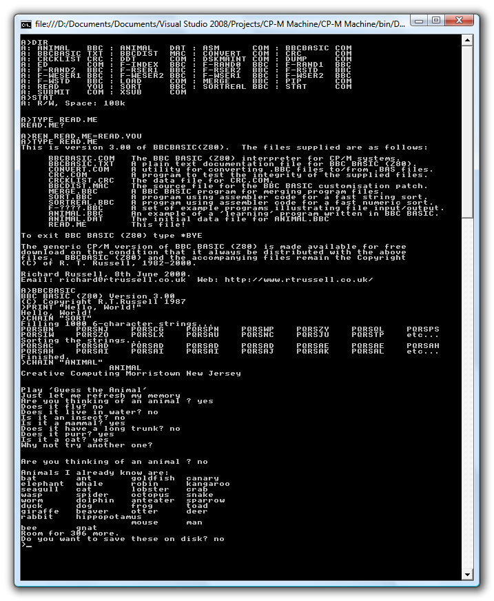
To turn this into a working bit of hardware, I intend to replace the C# part with a microcontroller to handle keyboard input, text output and interfacing to an SD card for file storage. It would also be responsible for booting the system by copying the OS to Z80 memory from the SD card. I'm not sure the best way to connect the microcontroller to the Z80, though; disk operations use DMA, which is easy enough, but for lighter tasks such as querying whether console input is available or outputting a character to the display it would be nice to be able to go via I/O ports. A couple of I/O registers may be sufficient as per the current design; a proper Z80 PIO would be even better if I can get my hands on one.
Of more concern is a suitable display; the above screenshot is from an 80-character wide display. Assuming a character was four pixels wide (which is about as narrow as they can be made whilst still being legible) imposes a minimum resolution of 320 pixels horizontally – my current LCD is only 128 pixels wide (not even half way there), and larger ones are really rather expensive!
Building a VGA line blanker and 3D glasses driver
Monday, 15th February 2010
Assembling a circuit on breadboard is a good way to experiment with electronics, but the result is not something you could really use – it's bulky, fragile and awkward to set up. It's far nicer to solder the components of the circuit together to form a more permanent device and put it in a enclosure to make it robust. This is not something I'm especially good at, but something I thought I'd try with the VGA line blanker and LCD shutter glasses controller I've been experimenting with recently.
In the past I've struggled along with a hand drill and the nail file on a Swiss Army knife, but have more recently acquired a high-speed rotary tool and an assortment of attachments which make things much easier. I took some photos when building this project, which I've documented below; I'm not sure my techniques are very efficient, but I do get there in the end. I'd be very glad to hear any advice anyone has!
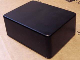
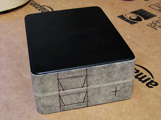
I started with a plain project box. Having planned roughly where I was going to put the VGA ports and DC power socket, I covered one side of the box in masking tape and drew on where I was going to put the holes.
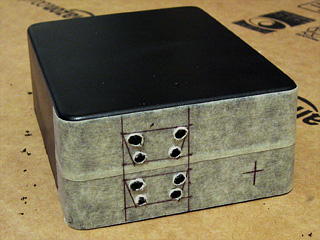
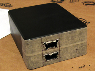
To cut straight-edged holes, such as those required for a D-subminiature connector, I drill a hole in each corner and use a small cylindrical burr to cut between the holes. This leaves a very rough edge, but is a good start.
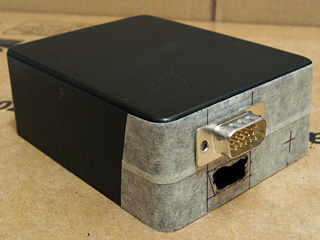
I then widen the hole using a large cylindrical burr and a needle file until the part I'm attempting to mount fits snugly.
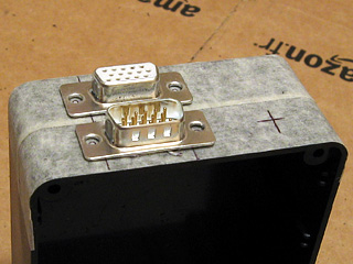
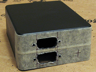
When I had both VGA connectors in place, I marked and drilled the holes for the jack posts that the VGA leads will screw into. Neither hole is especially neatly cut, but the D-subminiature connector overlaps the hole sufficiently to hide any shoddy workmanship.
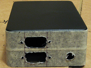
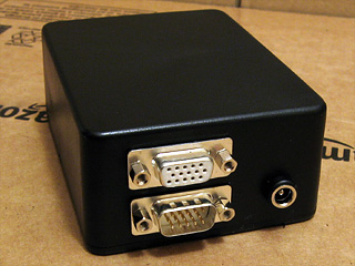
The last part of the back is the DC power socket. As I don't have a drill bit large enough to cut the hole on its own, I drill it as large as I can then widen it using the cylindrical burrs mentioned before. With all of the holes cut, I inserted the components to see how they look and identified one problem – I'd underestimated how fat the connectors on the end of VGA leads are. Fortunately, I have a slim VGA cable that fits, but a regular sized one does not – in future I'll need to remember to put the VGA connectors further apart!
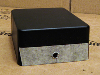
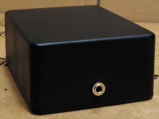
With that mistake fresh in my mind, I thought I'd move onto something a bit more difficult to get wrong – the 3.5mm stereo jack on the front of the box to plug the glasses into. This is just another round hole, cut in the same way as the DC power socket.
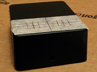
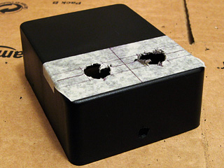
The two control switches on the top of the box require much larger holes. These were cut in the same way as before – a small hole is gradually widened by using a cylindrical burr. This is a very tedious job, not helped by having to keep stopping to clean the melted plastic that adheres to the burr.
Finally, the switches were installed. I was originally going to use latching push buttons, but had previously used those nice round rocker switches as the power switch on the AVR TV Game project so opted to use them instead.
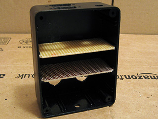
The final bit of physical work was to cut some stripboard down to size to fit inside the enclosure. These were cut by first scoring along the tracks where the cut was to be made, then snapping the board over the edge of a table. This results in a clean break, but to ensure a snug fit the boards were tidied up with a sanding drum. The lid (or, in my case, base) of the enclosure has a raised edge that fits inside the box, so the sanding drum was also used to remove two of the corners of the stripboard pieces to allow the base to fit.
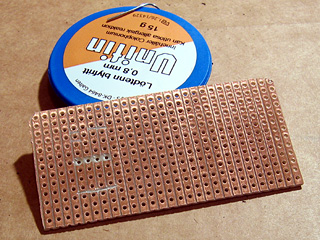
The next stage was to move onto the electronics, and I started with the circuit board that was to host the video amplifier IC, voltage regulator and Schmitt trigger on vsync/hsync. The video amplifier is attached to a TSSOP14 adaptor that has a D-shaped pin configuration, with two rows of four pins and two rows of three pins. Having cut through the tracks in the stripboard to mount the amplifier, I needed to find some suitable pin sockets.

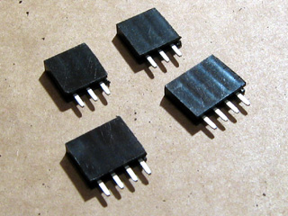
As I don't have any pin sockets with just three pins in them (only two, four and eight) I cut two eight-way pin sockets in two with a pair of wire cutters then tidied up the ragged edges with a sanding drum and needle file.
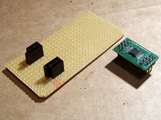
With the pin sockets soldered in place you can see the D shape I mentioned above. I don't generally plan stripboard circuits very thoroughly, preferring to start by placing large components in approximately the right location with respect to where the external connectors are and how they need to relate to other components. Once those are in place I add smaller components (such as discrete resistors or capacitors) before finishing by adding the wire links to connect all of the parts together. This does lead to situations where I wish that I'd placed a component one hole along to give myself more space or to avoid having to insert so many wire links, but it generally works.
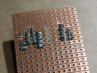
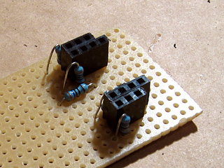
With the video amplifier in position, I added the resistors that are required on its inputs and outputs. To keep the circuit reasonably compact I cut through stripboard tracks between the holes using a conical HSS burr with a small tip – this is an especially useful tool when you need to deal with double-row pin sockets
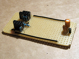
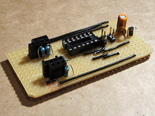
I then added the support circuitry for the voltage regulator (smoothing capacitors and a rectifier diode to protect the circuit if the polarity of the power supply is incorrect) and a socket for the Schmitt trigger IC. I find the easiest way to keep components in place on any sort of through-hole board is to tape them down firmly with masking tape before soldering – bending the legs out makes the parts much harder to remove if you make a mistake. Blu-Tack is easier to use but has a habit of melting when soldering and leaving an unpleasant blue residue on your circuit, so I'd advise against it! To make this part of the circuit slightly more future-proof a pair of jumpers are used to connect the sync lines (vsync and hsync) from the VGA input and VGA output together. These could be removed if I decided to change the logic board to override these signals – for example, as part of a sync-doubler, which injects a vsync pulse half way down the screen.
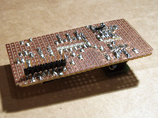
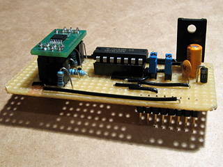
I finally added the bulkiest components; the 5V regulator and the pin header to connect the upper and lower boards together. Soldering pin headers to the underside of a board is a fiddly job, but is required in this instance to connect the bottom of the upper board to the top of the lower board.
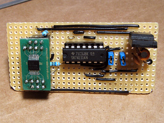
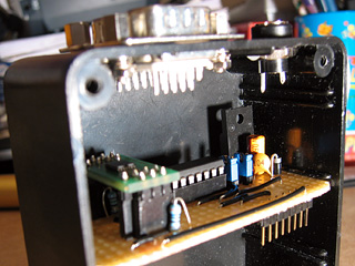
With the upper board completed it was time to put it into the enclosure and solder the VGA connectors and DC power socket to it. This is the part I least enjoy.
I started by soldering some stranded wire to the VGA connectors. Most of the wires are the same length, as they are required to carry signals to and from the circuit, but some wires are shorter and only connected to one of the VGA connectors. These are the white, yellow, orange and brown wires in the above photo, and these are attached to pins used to exchange information between the PC and the monitor (e.g. supported resolutions and refresh rates). As we're not interested in these, they're connected straight through from one connector to the other.
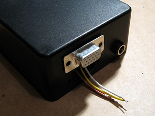
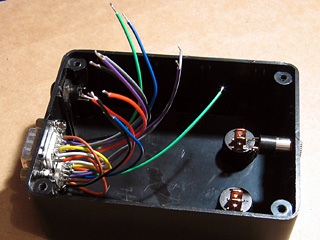
I inserted the VGA connector with these identification pins into the top hole, passed the shorter identification wires through the other and soldered them to the second VGA connector. This leaves the red, green, blue, vsync, hsync and ground pins loose inside, ready to be connected to the upper circuit board.
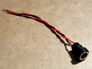
The DC power socket also needs to be connected to the circuit board, but at only two wires that's a much simpler job.
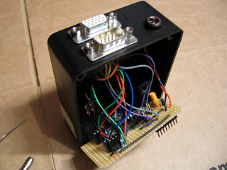
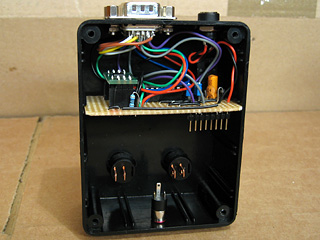
All of the loose leads are soldered onto the circuit board and stripboard is slotted into place inside the enclosure. The wires could be shorter, but that would have made soldering them a bit harder.
The lower circuit board will host the main logic for the project – it receives the vsync and hsync signals, and uses these to control whether the video signal should be blanked or not, and which shutter on the glasses should be closed and which should be open. It also contains the oscillator that generates the AC voltage that drives the glasses. I arranged the three logic ICs roughly next to eachother according to their layout on the breadboard version of the circuit and cut the stripboard tracks as appropriate.
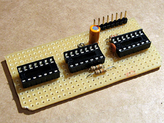
I started by adding the sockets for the ICs and pin header to connect this circuit board to the video amplifier one, then added the discrete components. As before, I taped the components down before soldering them in place to make the task easier. Being able to copy the circuit directly from the breadboard version also made the task much easier.
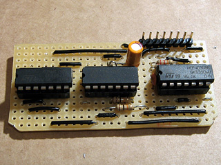
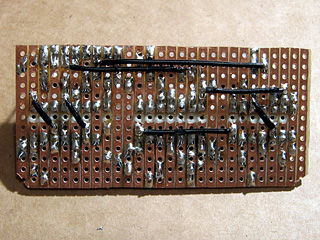
The last step for this part of the project was, as before, adding the wire links. Rather than run long wires around ICs I found it more practical to solder a few wires onto the underside of the stripboard.
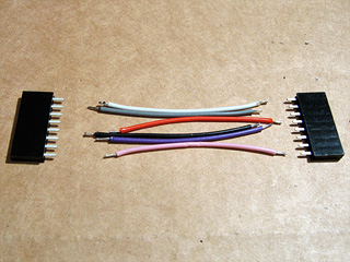
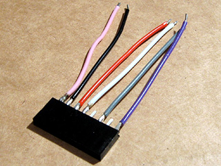
The two circuit boards needed to be connected together somehow. Without the facilities to make a proper ribbon cable, I just soldered some lengths of stranded wire (rather messily) between two pin sockets. As I'm not outputting anything to vsync or hsync (I'm feeding the input sync signals straight back to the output via the jumpers previously discussed), I didn't need to connect anything to these pins – hence the apparently missing wires in the photos.
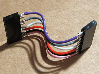
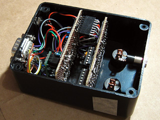
The cable to connect the two boards together needed to be bent to fit – it's getting snug, but everything's in there without having to be forced, which is a good sign.
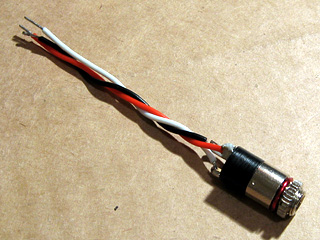
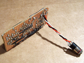
The next job was to attach the 3.5mm stereo jack that the LCD shutter glasses are plugged into. This is pushed through the hole in the enclosure from the inside and screwed on from the outside, so it can be soldered directly to the circuit board without having to thread it through the hole first. The small red "washer" is a length of enamelled wire that has been bent around the thread of the jack socket and is used as a spacer – without it, quite a lot of the thread protrudes from the front of the box, looking rather untidy.
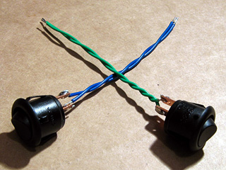
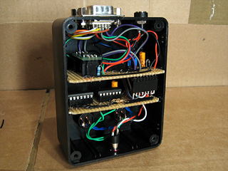
Last of all are the two control switches. These are soldered to the track side of the stripboard like the stereo jack, but must be snapped through their holes in the enclosure first, which is why they were left until last. Everything is slotted into place, the base of the enclosure is screwed on, and the project is pretty much complete.
The VGA cables don't fit especially well – the D-subminiature sockets are a bit too close to eachother. If I use a thin VGA extension cable and wiggle the leads I can just about get both to screw in.
The demonstration pattern from some previous ramblings of mine is quite useful for testing 3D glasses, and by holding the left eye of the shutter glasses to the screen you can see that only the "L" part of the image is let through.
3D glasses, a VGA line-blanker and fixing Quake
Wednesday, 3rd February 2010
Some time ago, I posted about using interlaced video to display 3D images. Whilst the idea works very nicely in theory, it's quite tricky to get modern video cards to generate interlaced video at a variety of resolutions and refresh rates. My card limits me to 1920×1080 at i30 or 1920×1080 at i25, and only lets me use this mode on my LCD when I really need it on a CRT. Even if you can coax the video card to switch to a particular mode, this is quite a fragile state of affairs as full-screen games will switch to a different (and likely progressively scanned) mode.
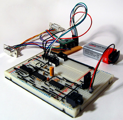
3D glasses adaptor with line blanker prototype
An alternative is to build an external bit of hardware that simulates an interlaced video mode from a progressive one. The easiest way of doing that is to switch off the RGB signals on alternate scanlines, blanking odd scanlines in one frame and even scanlines in the next. This type of circuit is appropriately named a line blanker, and my current implementation is shown above. It sits between the PC and the monitor, and uses a pair of flip-flops which toggle state on vsync or hsync signals from the PC. The output from the vsync flip-flop is used to control which eye is open and which is shut on the LCD glasses, and is also combined with the hsync flip-flop to switch the RGB signal lines on or off on alternate lines using a THS7375 video amplifier. Unfortunately, this amplifier is only available as TSSOP, which isn't much fun to solder if you don't have the proper equipment; I made a stab at it with a regular iron, the smallest tip I could find, lots of no-clean flux and some solder braid. I have been informed that solder paste makes things considerably easier, so will have to try that next time.
My cheap LCD glasses lack any form of internal circuitry, merely offering two LCD panels wired directly to a 3.5mm stereo jack, and so I'm using the 4030 exclusive-OR gate oscillator circuit to drive them.
The adaptor provides one switch to swap the left and right eyes in case they are reversed, and another is provided to disable the line blanking circuit (useful for genuine interlaced video modes or alternate frame 3D). You can download a schematic of the circuit here as a PDF.
I've been using these glasses to play Quake in 3D, which is good fun but an experience that was sadly marred by a number of bugs and quirks in Quake's 3D mode.
WinQuake, demonstrating the crosshair bug and excessive stereo separation of the weapon
The most obvious problems in the above screenshot are the migratory crosshair (appearing 25% of the way down the screen instead of vertically centred) and the excessive stereo separation of the player's weapon.
If the console variable LCD_X is non-zero, Quake halves the viewport height then doubles what it thinks is the stride of the graphics buffer. This causes it to skip every other scanline when rendering. Instead of rendering once, as normal, it translates the camera in one direction, renders, then offsets the start of the graphics buffer by one scanline, translates the camera in the other direction then renders again. This results in the two views (one for each eye) being interleaved into a single image.
The crosshair is added after the 3D view is rendered (in fact, Quake just prints a '+' sign in the middle of the screen using its text routines), which explains its incorrect position – Quake doesn't take the previously halved height of the display into consideration, causing the crosshair to be drawn with a vertical position of half of half the height of the screen. That's pretty easy to fix – if LCD_X is non-zero, multiply all previously halved heights and Y offsets by two before rendering the crosshair to compensate.
WinQuake, demonstrating the DirectDraw corruption bug
A slightly more serious bug is illustrated above. When using the DirectDraw renderer (the default in full-screen mode), the display is corrupted. This can be fixed by passing -dibonly to the engine, but it would be nice to fix it.
After a bit of digging, it appeared that the vid structure, which stores fields such as the address of the graphics buffer and its stride, was being modified between calls to the renderer. It seemed to be reverting to the actual properties of the graphics buffer (i.e. it pointed to the top of the buffer and stored the correct stride of the image, not the doubled one). Further digging identified VID_LockBuffer() as the culprit; this does nothing if you're using the dib rendering mode, but locks the buffer and updates the vid structure in other access modes. Fortunately, you can call this function as many times as you like (as long as you call VID_UnlockBuffer() a corresponding number of times) – it only locks the surface and updates vid the first time you call it. By surrounding the entire 3D rendering routine in a VID_LockBuffer()…VID_UnlockBuffer() pair, vid is left well alone, and Quake renders correctly in full-screen once again.
The final issue was the extreme stereo separation of the player weapon, caused by its proximity to the camera – it does make the game quite uncomfortable to play. The game moves the camera and weapon to the player's position, then applies some simple transformations to implement view/weapon bobbing, before rendering anything. Applying the same camera offset and rotation to the player weapon as the camera when generating the two 3D views put the weapon slap bang in the middle of the screen, as it would appear in regular "2D" Quake. This gives it the impression of a carboard cutout, and can put it behind/"inside" walls and floors when you walk up to them; I've added a console variable, LCD_VIEWMODEL_SCALE, that can be used to interpolate between the default 3D WinQuake view (value: 1) and the cardboard cutout view (value: 0).
WinQuake with the 3D fixes applied
You can download the replacement WinQuake from here – you can just overwrite any existing executable. (You will also need the VC++ 2008 SP1 runtimes, if you do not already have them). Source code is included, and should build in VC++ 2008 SP1 (MASM only appears to be included in SP1, which is required to compile Quake's extensive collection of assembly source files).
If you don't have a copy of Quake, I recorded its looping demos in 3D and uploaded them to YouTube. This was before I made the above fixes, so there's no crosshair or player weapon model in the videos – if you have access to YouTube-compatible 3D glasses or crossable eyes, click here. 
Ejecting discs from a damaged camcorder with a remote control
Tuesday, 29th December 2009
I hope that those of you who celebrate it had a good Christmas break and will have an excellent new year!
I recently attempted to repair a DVD camcorder that had been dropped; the eject button no longer worked, though the disc could be ejected by connecting to camera to a PC, right-clicking the DVD drive that subsequently appears in Explorer, then selecting Eject.
I started by removing all of the screws around the affected area, but the plastic casing remained strongly held together by some mysterious internal force. I removed more and more screws, but it soon became apparent that the only way to get into the camera would be to force it open – not being my camera, I didn't feel comfortable doing so, as the rest of the camera worked well and I didn't want to damage any fragile internal mechanisms. I couldn't find any dismantling guides online, so gave up on the idea of fixing the button.
Fortunately, I own the same model of camcorder – a Panasonic VDR-D250 – myself. With my interest in infrared remote controls I had previously found information about the Panasonic protocol it uses. The supplied remote control only has a few simple buttons on it (no eject button, sadly), but I reckoned that the camcorder may accept a number of other commands that the stock remote didn't include.
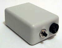
I started by modifying a universal remote control program for the TI-83+ that I had previous written to allow me to send specific commands to the camcorder, then ran through all of the possible command IDs, noting down those that appeared to have some effect. Eventually I had a pretty decent list, albeit one with quite a few gaps in it. Fortunately, I had found the Eject button code, along with codes to switch mode (which is done on the camera by rotating a mode dial), one that powers the camcorder off, another that appears to restart the camera and another one that resets all settings (not so useful, that one).
Having found the eject code, I set about building a dedicated remote control. I picked the ATtiny13 microcontroller as a base, as that's a more than capable microcontroller with its 9.6MHz internal clock, 1KB program memory, 64 bytes SRAM and 3V operation.
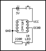
I was a bit surprised to see that AVR-GCC supports the ATtiny13, and whilst C may seem overkill for such a project I'll gladly take advantage of anything that makes my life easier.
// Requisite header files.
#include <avr/io.h>
#include <util/delay.h>

// Frequency of the IR carrier signal (Hertz).
#define F_IR_CARRIER (37000)

// Timing of the data bits (microseconds).
#define T_DX_MARK   (440)
#define T_D0_SPACE  (440)
#define T_D1_SPACE (1310)

// Timing of the lead-in and lead-out bits (microseconds).
#define T_LEAD_IN_MARK    (3500)
#define T_LEAD_IN_SPACE   (1750)
#define T_LEAD_OUT_MARK    (440)
#define T_LEAD_OUT_SPACE (74000)

// Commands definitions.
#define OEM_DEVICE_1_CODE         (2)
#define OEM_DEVICE_2_CODE        (32)
#define CAMCORDER_DEVICE_ID     (112)
#define CAMCORDER_SUB_DEVICE_ID  (40)
#define CAMCORDER_COMMAND_EJECT   (1)

// Transmits a single unformatted byte.
void panasonic_send_byte(uint8_t value) {
    // Send eight data bits.
    for (uint8_t bit = 0; bit < 8; ++bit, value >>= 1) {
        // Send the mark/burst.
        DDRB |= _BV(1);
        _delay_us(T_DX_MARK);
        // Send the space.
        DDRB &= (uint8_t)~_BV(1);
        _delay_us(T_D0_SPACE);
        // Extend the space if it's a "1" data bit.
        if (value & (uint8_t)1) {
            _delay_us(T_D1_SPACE - T_D0_SPACE);
        }
    }
}

// Transmits a formatted command packet to the IR device.
void panasonic_send_command(uint8_t oem_device_code_1, uint8_t oem_device_code_2, uint8_t device_code, uint8_t sub_device_code, uint8_t command) {
    // Send the lead in.
    DDRB |= _BV(1);
    _delay_us(T_LEAD_IN_MARK);
    DDRB &= (uint8_t)~_BV(1);
    _delay_us(T_LEAD_IN_SPACE);

    // Send the five command bytes.
    panasonic_send_byte(oem_device_code_1);
    panasonic_send_byte(oem_device_code_2);
    panasonic_send_byte(device_code);
    panasonic_send_byte(sub_device_code);
    panasonic_send_byte(command);

    // Send the checksum.
    panasonic_send_byte(device_code ^ sub_device_code ^ command);

    // Send the lead out.
    DDRB |= _BV(1);
    _delay_us(T_LEAD_OUT_MARK);
    DDRB &= (uint8_t)~_BV(1);
    _delay_us(T_LEAD_OUT_SPACE);
}

// Main program entry point.
int main(void) {

    TCCR0A |= _BV(COM0B0) | _BV(WGM01);     // Toggle OC0B when on CTC reload. Use CTC mode.
    TCCR0B |= _BV(CS00);                    // Set clock source to CPU clock/1.
    OCR0A = (F_CPU / F_IR_CARRIER / 2) - 1; // Set the CTC reload value to generate an IR signal at the correct carrier frequency.

    // Send the "eject" command ad infinitum.
    for(;;) {
        panasonic_send_command(OEM_DEVICE_1_CODE, OEM_DEVICE_2_CODE, CAMCORDER_DEVICE_ID, CAMCORDER_SUB_DEVICE_ID, CAMCORDER_COMMAND_EJECT);
    }
}
The code is about as simple as the circuit. IR signals are transmitted as carefully timed bursts of a particular carrier frequency (37kHz in this case). For example, to send a "0" bit 440μS of this 37kHz signal are sent followed by 440μS of silence. To send a "1" bit, 440μS of carrier signal are sent as before, but a 1310μS period of silence follows it.
The AVR's timer is used to generate a ~37kHz carrier signal. The timer is an eight-bit counter that counts up at a user-defined rate (in my case I've chosen to increment the counter by one every CPU clock cycle). I've configured it to invert the output level of pin OC0B and reset every time it hits a particular value. By setting whether this pin is an output or an input the output of a burst of 37kHz IR signal or silence can be selected. Simple delay loops, generated with the helper function _delay_us, are used to time the transmission of data bits.
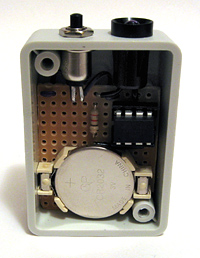
The final step was to assemble the circuit on stripboard and install it in a smallish project box. I've put the switch adjacent to the LED for two reasons; to conserve space and to protect it a little from accidentally being pressed by the protruding LED bezel.
Building a single-button remote control is a relatively straightforward affair, so whilst the above code has a very specific purpose it should be easy enough to modify it to control other devices.
Playing VGMs on an STM8S
Monday, 14th December 2009
Following the STM8S tutorial in my previous post, I've tried to put the chip to some practical use. My initial experiments into producing a video signal proved unsuccessful; I managed a static image using hard-coded delay loops, but when trying to use interrupts to trigger the generation of scanlines the timing was all wrong and without an oscilloscope or a working simulator I couldn't find out what was wrong. I decided to turn my attention from picture to sound.
VGM files store game music by logging the data written to the sound chips inside the console or computer directly along with the delay between writes. This results in reasonably small files that are capable of producing excellent sound quality, depending on the way the sound chips are emulated (or, in some cases, not emulated).
I've chosen to focus on the SN76489, a simple sound chip found in a variety of machines including the Sega Master System and BBC Micro. Three of its four sound channels are simple square wave tones, implemented as a 12-bit decrementing counter that flips the state of its output every time it underflows and is reset. Changing the value that is preloaded into the counter when it is reset changes the period of the output square wave, resulting in a change of pitch.
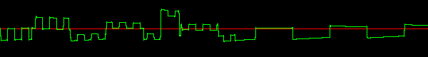
The fourth channel proves rather more of a challenge. It uses a shift register (15- or 16-bit depending on the particular version of the chip) instead of a simple tone counter, and has two modes. When generating periodic noise a single bit shuttles around the shift register, generating a 1/15th or 1/16th duty cycle square wave. This has effect of producing a lower pitch with a distinctive "buzzy" timbre. The other mode is white noise, which uses a feedback system to generate pseudo-random noise.
The emulated SN76489, or PSG, has been implemented in two parts. The first is an interrupt handler written in STM8S assembly for speed. This is executed approximately 44,100 times a second (44.1kHz is the internal time step used in VGM files) and is used to update the internal PSG counters and shift register and generate the output level for that particular sample. Two output levels are generated as I've implemented the Game Gear's stereo extension to the PSG (this simply lets you switch individual channels on or off for each ear). These levels are loaded into capture compare registers for TIM2, which is used in PWM mode to generate the analogue output signals.
The rest of the code is written in C. This includes the second part of the emulated PSG, which handles bytes written to the PSG and updates its internal registers as appropriate.
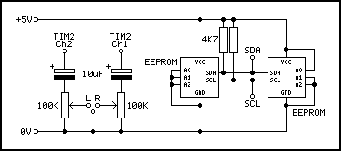
Due to a 16KB limitation with the free version of the Cosmic compiler (and the 32K physical limitation of the microcontroller itself) the VGM file is stored on external EEPROMs which are accessed over the I2C bus via the microcontroller's I2C peripheral. As I don't have any large single EEPROMs, I've used two 32KB EEPROMs, one at address 0xA0 and the other at 0xA2. When the read pointer overflows one EEPROM it automatically steps to the next EEPROM. In theory any size could be supported using this code, but I've used 16-bit variables for all of the file pointers introducing a 64KB limit – this should be easily fixable, but I don't own enough memory to test the code myself, so I've left it as it is for the moment.
// The program I use to split VGM files into 32KB chunks.
// Bear in mind that most VGMs are compressed (VGZ): you'll need to decompress them first.
// You can use 7-zip to do so.
using System.IO;
class Program {
    static void Main(string[] args) {
        var SourceFile = @"D:\Documents\Documents\VGM\StrykersRun-title";
        using (var r = new BinaryReader(File.OpenRead(SourceFile))) {
            for (var i = 0; i < int.MaxValue; ++i) {
                var data = r.ReadBytes(32 * 1024);
                if (data.Length == 0) break;
                File.WriteAllBytes(string.Format("{0} [{1}].bin", Path.GetFileNameWithoutExtension(SourceFile), i), data);
            }
        }
    }
}
To take advantage of the delay between PSG accesses I've implemented a very simple buffering system that queues up a few bytes in advance from the EEPROM. This works well for music, but sampled audio (which involves updating the PSG very rapidly) doesn't work as the code spends too much time waiting for data to be transferred from the EEPROMs.
I've included some recordings of the output below.
- Firetrack (Nick Pelling, BBC Micro)
- Stryker's Run (Martin Galway, BBC Micro)
- Alien 3 – Episode 2 (Matt Furniss, Sega Master System)
- Sega Chess – White Wins (Matt Furniss, Sega Master System)
- Gunstar Heroes – Military on the Max-Power (Kazuo Hanzawa, Hitoshi Sakimoto, M.Yuzuno, M.Yoshida, Y.Mizusawa; Sega Game Gear) [Stereo]
- That Other Final Conflict (RushJet1)
- Alex Kidd: The Lost Stars – I'm the Miracle Ball (Sega Master System) [Sampled speech, doesn't work]
The source code can be downloaded from here. If you do try to run it you'll find that it tends to hang when trying to initialise the EEPROM; this is due to the I2C bus being left in an active state by forcefully terminating the program before debugging. I find it helps to program the board, disconnect then reconnect the power supply to the EEPROMs to reset them, then hitting continue in the debugger.
STM8S-Discovery review and tutorial
Thursday, 3rd December 2009
STMicroelectronics recently released the STM8S-Discovery, an exceedingly cheap (RRP $7) evaluation kit for one of their 8-bit microcontrollers. It features the microcontroller itself (an STM8S105C6), running at up to 16MHz and offering 32KB of program memory, 2KB of RAM and 1KB of data EEPROM. This microcontroller has a solid set of on-board peripherals, including four timers (one advanced, one general-purpose, and one basic), SPI, I2C, UART, and ADC – so there are plenty of connectivity options. The device offers up to 38 general-purpose I/O pins.
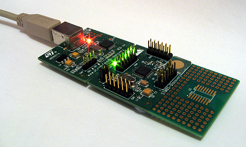
The evaluation board is pretty feature-packed, and includes an integrated ST-LINK for programming and debugging over USB. The circuit board has been designed so that you can simply snap off the ST-LINK part if you'd like to use the microcontroller on its own. Standard 0.1" pin headers are provided to permit you to connect the board to other components, and a small wrapping area is also present. A jumper can be used to select 5V or 3.3V operation.
A green LED and a touch sensitive key are built into the evaluation board; the device comes pre-programmed with a demo program that flashes this LED at different rates when you touch the key.
All in all, a decent piece of kit – but what really sets it apart is its price. ST's recommended price is $7; I bought mine for £4.25 from Farnell. All you need to do is provide a USB A to USB B cable and download the various development tools (Windows only at the time of writing), datasheets and libraries.
 First impressions
I really wasn't expecting much for £4.25, but am very impressed with the hardware. It's solidly built and comes attractively packaged, with clear instructions on the back of the box on how to run the demo program (just plug it in to a USB port!) and where to go next for development tools.
Unfortunately, what appears to be lacking at the moment – not surprisingly for a new product – is guidance for absolute beginners with ST's microcontrollers. Hopefully that will improve as more people get hold of these new kits, as their incredibly low price and self-contained nature makes them ideal for beginners (no need to build up a collection of parts or buy a programmer to get started, just plug and play). I personally found the documentation quite baffling, and judging by a thread on Hack a Day I wasn't the only one.
Disclaimer
I'm not an expert with ST's microcontrollers, but I have at least managed to get something running on the microcontroller after a few frustrating hours spent with the current documentation. The following code may not be the best, but it is simple and it should work (if I've missed anything out or not been clear enough anywhere, please let me know so I can fix it). It doesn't go into any great detail; my assumption is that if you can get some code you've written yourself running on your evaluation board and understand how to use the basic peripherals offered by the microcontroller to work with the board's LED and touch key you should be ready enough to dive into the official documentation and sample code yourself!
Getting started
If you visit the STM8S-Discovery page, you will see options to download various pieces of software and development tools. You'll need to download the following:
- A C compiler (I'm currently using Cosmic's, but it's worth installing the Raisonance compiler too).
- The ST MCU Toolset, which includes the ST Visual Develop IDE.
- The application development package (this contains examples and relevant libraries to access the various peripherals of the chip).
- The STM8S105C6 datasheet (invaluable device specifications/information).
- The STM8S microcontroller family reference manual (a general overview of the STMS8 family, including documentation on the various on-board peripherals).
- The STM8S-Discovery evaluation board user manual (information specific to the evaluation board, including circuit diagrams and other specifications).
There is a document that accompanies the development package, Developing and debugging your STM8S-DISCOVERY application code, which contains instructions on setting up a project – confusingly, these directions don't appear to apply to Raisonance's tool chain, and rely on copying and pasting files from the demo programs. You will need to register the compilers to be able to use them, and Cosmic's registration process is handled by a human so may take some time for you to receive your licence key.
Debugging one of the sample programs
One way to verify that everything is set up correctly and to try out the development tools is to build one of the sample programs included as part of the application development package. In this zip file you will find a directory named STM8S-Discovery_dev; extract this somewhere sensible. Run ST Visual Develop, and select File→Open Workspace. Open the file STM8S-Discovery_dev\Project\Discover\STVD\Cosmic\Discover.stw – this is the project that came pre-loaded onto the evaluation board. If you click Build→Build it should crunch away and after a few seconds should report that there were no errors.
We'll now need to set up the IDE to use your evaluation board's ST-LINK as its debugging instrument. Click Debug instrument→Target Settings and select Swim ST-Link in the dropdown. You can leave the other settings as they are; click OK to close the dialog.
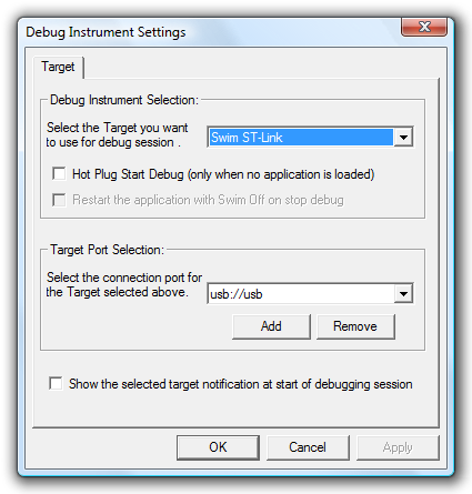
If you now click Debug→Start Debugging (or the blue "D" in the toolbar) the IDE should program the evaluation board and then enter the debugger in "Break" mode. Press Continue (F5) to start running the program; at this point you should be able to use the touch sensitive key on the board to change the rate at which the green LED flashes. When you're done, click Debug→Stop Debugging (or the red cross button in the toolbar) to stop debugging.
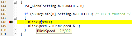
The debugger shouldn't be especially surprising to anyone who has used a graphical debugger (e.g. Visual Studio) before. Try going to line 148 in main.c – BlinkSpeed++; – and selecting Edit→Insert/Remove Breakpoint. Start debugging as before, and you'll notice that when you touch the key this time the debugger breaks on that line. Click Debug→Continue and the program will continue. Marvellous – all pretty intuitive thus far.
Creating your own project
Creating your own project is a rather more involved process, as there's quite a lot you need to set up first. Hopefully this step-by-step guide should help!
- Firstly, click File→New Workspace, and select Create Workspace and Project from the dialog that appears.
- Now, we need to store our workspace (analagous to a solution in Visual Studio) somewhere; create a new directory for the workspace that is preferably not inside Program Files and give the workspace a name. I'm going to go for "Blinkenlight" as my workspace name.
- Create a new project with the same name as the solution name. It should default to the same directory; keep this as it is. Select STM8 Cosmic as the toolchain.
- Select STM8S105C6 as the microcontroller.
With that done, you should have a shiny new workspace and project containing two files – main.c, containing the entry point for your application, and stm8_interrupt_vector.c, used to associate interrupt requests with interrupt service routines – more on those later. If you build the project and try to debug it you'll note that it does precisely nothing of use. Let's make it do something useful!
Adding the standard firmware library
To access the various peripherals of the microcontroller, ST have provided an extensive standard firmware library. You will need to download this from the STM8S documents and files page; it's the zip archive named STM8S firmware library. Open the zip archive, and copy the FWLib\library folder to your own project folder. You may wish to rename the library folder FWLib, so you should end up with the two folders Project\FWLib\inc and Project\FWLib\src.
There is a folder named project in the firmware library download – copy stm8s_conf.h from this folder into the root of your project folder.
Now, return to ST Visual Develop. Use the workspace panel to the left to create two new folders in your project – Source Files\FWLib and Include Files\FWLib. Add all of the files from FWLib\inc to Include Files\FWLib and stm8s_conf.h to the root of Include Files. You should now have something that looks like this:
You will also need to inform the firmware library that you are using an STM8S105 microcontroller as opposed to the default STM8S208. Here are two ways of doing this – pick whichever seems easiest to you.
- Open stm8s.h in Project\FWLib\inc, comment out #define STM8S208 and uncomment #define STM8S105 near the top of the file.
- Pass the definition directly to the compiler by clicking Project→Settings, selecting the C Compiler tab and typing STM8S105 into the Preprocessor Definitions field. You will need to do this twice; once for the Debug configuration and once for Release (select the configuration with the drop-down box in the top left).
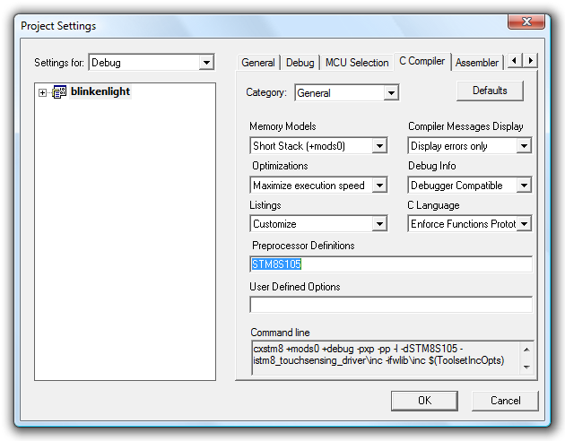
Illuminating the LED using GPIO
The cathode of the evaluation board's LED is connected to PD0 on the microcontroller – that is, pin 0 of port D. By driving this pin low we could therefore illuminate the LED. If you consult the documentation for the standard firmware library – it's the stm8s_fwlib_um.chm file in the zip archive – you can see a number of helper functions dedicated to GPIO, or "general-purpose I/O". To use the GPIO functions, we need to do two things:
- Add FWLib\src\stm8s_gpio.c to the project under Source Files\FWLib.
- Enable inclusion of the relevant GPIO header files, achieved by uncommenting #define _GPIO (1) in stms8_conf.h
Both steps will need to be carried out whenever you want to use a new peripheral (e.g. a timer or the UART). Once that's done, you can modify main.c to read as follows:
#include "stm8s.h"

int main(void) {

    // Reset ("de-initialise") GPIO port D.
    GPIO_DeInit(GPIOD);

    // Initialise pin 0 of port D by setting it as:
    // - an output pin,
    // - using a push-pull driver,
    // - at a low logic level (0V), and
    // - 10MHz.
    GPIO_Init(GPIOD, GPIO_PIN_0, GPIO_MODE_OUT_PP_LOW_FAST);

    // Infinite loop.
    for(;;);
}
There are more comments than code there – using the firmware library makes life rather easy, once it's set up! If you start debugging that, you'll note that the LED does indeed light up. It's not much, but it's a sign of life.
Flashing the LED using a delay loop
The GPIO library provides a handy GPIO_WriteReverse() function, which inverts the state of a pin. By toggling PD0, we can make the LED flash. To slow this flashing down at a rate we can see, a delay loop is introduced that delays for 50,000 nops, plus overhead of the for loop structure, between calls to GPIO_WriteReverse().
#include "stm8s.h"

int main(void) {

    // Reset ("de-initialise") GPIO port D.
    GPIO_DeInit(GPIOD);

    // Initialise pin 0 of port D.
    GPIO_Init(GPIOD, GPIO_PIN_0, GPIO_MODE_OUT_PP_LOW_FAST);

    // Infinite loop.
    for(;;) {

        // Delay for a short while.
        u16 d;
        for (d = 0; d < 50000; ++d) {
            // Without a nop() in here, the entire loop would be optimised away!
            nop();
        }

        // Invert the LED pin's state to flash it.
        GPIO_WriteReverse(GPIOD, GPIO_PIN_0);
    }
}
The reason for the nop() is that without it, the compiler optimises away the entire for loop as it does nothing useful.
Well, that's a bit more dynamic, but surely there's a better way to do this than a hard-coded delay loop?
Timers
Timers – of which the STM8S has four with varying capabilities – are an extremely versatile peripheral. They are typically based around a counter, which counts up or down, and various events can be triggered when this counter reaches particular values. We'll start here by using the TIM3 peripheral.
To use TIM3 we need to perform the following steps, as we did previously for GPIO:
- Add FWLib\src\stm8s_tim3.c to the project under Source Files\FWLib.
- Uncomment #define _TIM3 (1) in stms8_conf.h
By default, the microcontroller uses its internal 16MHz RC oscillator ("HSI", or high-speed internal) divided by eight as a clock source. This results in a base timer frequency of 2MHz. When configuring a timer, you can specify a prescaler to further divide the clock frequency – if you were to divide the 2MHz clock frequency by 2000, the timer would count up once every millisecond.
TIM3 restricts the prescaler to powers of two between 1 and 32,768, so we'll use a prescaler of 2048 (that's close enough for jazz). You also need to specify a timer period; this is the value up to which the timer will count before resetting itself. With a period of 999, the timer will run from 0 to 999 before resetting – approximately one thousand milliseconds, or one second, from start to finish.
// Reset ("de-initialise") TIM3.
TIM3_DeInit();

// Set TIM3 to use a prescaler of 2048 and have a period of 999.
TIM3_TimeBaseInit(TIM3_PRESCALER_2048, 999);

// Enable TIM3.
TIM3_Cmd(ENABLE);
Using the standard firmware library allows for easy timer configuration. Now that we have a timer running, we can query its counter value to flash the LED – if it's in the range 0~499, switch the LED on; if it's in the range 500~999, switch the LED off. Building on the ealier source code, here's a program that does just that:
#include "stm8s.h"

int main(void) {

    // Reset ("de-initialise") GPIO port D.
    GPIO_DeInit(GPIOD);
    // Initialise pin 0 of port D.
    GPIO_Init(GPIOD, GPIO_PIN_0, GPIO_MODE_OUT_PP_LOW_FAST);

    // Reset ("de-initialise") TIM3.
    TIM3_DeInit();
    // Set TIM3 to use a prescaler of 2048 and have a period of 999.
    TIM3_TimeBaseInit(TIM3_PRESCALER_2048, 999);
    // Enable TIM3.
    TIM3_Cmd(ENABLE);

    // Infinite loop.
    for(;;) {
        if (TIM3_GetCounter() < 500) {
            // Output a low on the LED pin to illuminate it.
            GPIO_WriteLow(GPIOD, GPIO_PIN_0);
        } else {
            // Output a high on the LED pin to switch it off.
            GPIO_WriteHigh(GPIOD, GPIO_PIN_0);
        }
    }
}
Pulse-width modulation for flashing
One of the many features of these timers is the ability to generate pulse-width modulation – PWM – output on dedicated pins. When this feature is enabled, the timer will set the output pin to one logic level when it starts or restarts and to another when it reaches a used-defined threshold. This is effectively what we're doing in our current program, just manually – far better if the timer could do it for us automatically!
The green LED is connected to PD0, which also acts as TIM3_CH2, or TIM3's channel 2. We can remove most of the code from our previous program, including the GPIO code, leaving us with the following:
#include "stm8s.h"

int main(void) {

    // Reset ("de-initialise") TIM3.
    TIM3_DeInit();

    // Set TIM3 to use a prescaler of 2048 and have a period of 999.
    TIM3_TimeBaseInit(TIM3_PRESCALER_2048, 999);

    // Initialise output channel 2 of TIM3, by setting:
    // - PWM1 mode (starts activated, deactivates when capture compare value is hit),
    // - output is enabled,
    // - capture compare value of 500, and
    // - an active signal is low (0V).
    TIM3_OC2Init(TIM3_OCMODE_PWM1, TIM3_OUTPUTSTATE_ENABLE, 500, TIM3_OCPOLARITY_LOW);

    // Enable TIM3.
    TIM3_Cmd(ENABLE);

    // Infinite loop.
    for(;;);
}
In PWM1 mode, the output starts in the activated state. As we have specified that TIM3_OCPOLARITY_LOW is an activated state, this means that the output will start at a logic low (the LED will be illuminated). When the capture compare value (500) is reached, the output will switch to the deactivated state (logic high) and the LED will switch off. If you run this program as before you will see that the LED does indeed flash on and off automatically.
Pulse-width modulation to change brightness
As the LED is on for approximately 500ms and off for approximately 500ms it is on half of the time. On average, therefore, it is at half its possible brightness. If you modify the 500 in the TIM3_OC2Init function call to 250 and run the program again you will see that on for a quarter of the possible time, and at 750 it is on for three quarters of the possible time. By increasing the rate at which the LED flashes so that it appears to be continuously lit we can control its apparent brightness by adjusting the relative amount of time it is switched on in comparison to the time it is switched off.
We can increase the rate at which the LED flashes by reducing the prescaler of TIM3. Try changing the TIM3_TimeBaseInit call to use TIM3_PRESCALER_16 instead of TIM3_PRESCALER_2048, and change the capture compare value in the TIM3_OC2Init call to 100. When you run your program, the LED on the board will appear to be dimly lit. If you pick up the board and very carefully shake it from side to side you should be able to see that the LED is flashing from the dotted trace it leaves in the air. If you drop the prescaler all the way down to TIM3_PRESCALER_1 you will find that you have to shake the board much faster, but take care not to damage anything!
The brightness of the LED can be modified at runtime by changing the value of the capture compare register with the TIM3_SetCompare2 function.
#include "stm8s.h"

// Short delay loop.
void delay(void) {
    u16 d;
    for (d = 0; d < 150; ++d) {
        nop();
    }
}

int main(void) {

    // Reset ("de-initialise") TIM3.
    TIM3_DeInit();

    // Set TIM3 to use a prescaler of 1 and have a period of 999.
    TIM3_TimeBaseInit(TIM3_PRESCALER_1, 999);

    // Initialise output channel 2 of TIM3.
    TIM3_OC2Init(TIM3_OCMODE_PWM1, TIM3_OUTPUTSTATE_ENABLE, 0, TIM3_OCPOLARITY_LOW);

    // Enable TIM3.
    TIM3_Cmd(ENABLE);

    // Infinite loop.
    for(;;) {

        u16 brightness;

        // Set the brightness from 0 to 999 in a loop (fade up).
        for (brightness = 0; brightness < 1000; ++brightness) {

            // Set the brightness of the LED by modifying the capture compare register
            // for TIM3's channel 2.
            TIM3_SetCompare2(brightness);

            // Delay a short while.
            delay();
        }

        // Set the brightness from 1000 to 1 in a loop (fade down).
        for (brightness = 1000; brightness > 0; --brightness) {

            // Set the brightness of the LED.
            TIM3_SetCompare2(brightness);

            // Delay a short while.
            delay();
        }
    }
}
The above program fades the LED up from the minimum brightness to the maximum brightness then back down again in an infinite loop. It also reintroduces our old enemy, the delay loop, which leads us neatly on to the next subject – interrupts.
Interrupts
Interrupts provide a way to respond to events in a way that doesn't require that we constantly check (poll) the event source. One such event is a timer overflowing – we can use this event to update the brightness of the LED every millisecond without having to poll a timer's counter manually or use delay loops.
We'll use TIM1 to generate the interrupt; it provides a few additional features that are not present on the other timers, but we'll need to keep TIM2 and TIM4 free for later. As before, you'll need to add stm8s_tim1.c to your project and uncomment #define _TIM1 (1) in stm8s_conf.h.
We'll start by adding some skeleton interrupt handler code and reference it in the interrupt vector table to ensure that it is called when the timer updates itself. Firstly, add the two following files to your project:
stm8s_it.c
#include "stm8s.h"
#include "stm8s_it.h"

void TIM1_UPD_OVF_TRG_BRK_IRQHandler(void) {
    // TODO: Implement TIM1 update interrupt handler.
}
stm8s_it.h
#ifndef __STM8S_IT_H
#define __STM8S_IT_H

@far @interrupt void TIM1_UPD_OVF_TRG_BRK_IRQHandler(void);

#endif
These stm8s_it files contain the interrupt request handlers. Interrupt handler functions are called via the interrupt vector table, which is defined in the stm8_interrupt_vector.c file that was automatically generated when you created the project. Open this file and add #include "stm8s_it.h" to the top of it so that it can see your interrupt handler functions. According to the STM8S105xx datasheet the TIM1 update/overflow interrupt is mapped to IRQ 11, so scroll down the table of interrupt vectors and change NonHandledInterrupt on the line marked irq11 (some lines omitted for clarity):
struct interrupt_vector const _vectab[] = {
    {0x82, (interrupt_handler_t)_stext}, /* reset */
    {0x82, NonHandledInterrupt}, /* trap  */
    {0x82, NonHandledInterrupt}, /* irq0  */
    /* [...] */
    {0x82, NonHandledInterrupt}, /* irq10 */
    {0x82, (interrupt_handler_t)TIM1_UPD_OVF_TRG_BRK_IRQHandler}, /* irq11 */
    {0x82, NonHandledInterrupt}, /* irq12 */
    /* [...] */
    {0x82, NonHandledInterrupt}, /* irq29 */
};
Now we have that in place we can start writing the interrupt handler code. Internally, interrupts are signalled by setting a flag in a control register, which the microcontroller periodically checks. If you do not clear this flag the microcontroller will call your interrupt handler again as soon as you return from the function, so you must remember to do so – this is done with the TIM1_ClearITPendingBit(TIM1_IT_UPDATE) function. Using a variable to store the current brightness "direction" (positive to get brighter; negative to get dimmer) the LED brightness could be adjusted every time the timer overflowed using the following code:
stm8s_it.c
#include "stm8s.h"
#include "stm8s_it.h"

s16 brightness_direction = +1; // Start by getting brighter.

void TIM1_UPD_OVF_TRG_BRK_IRQHandler(void) {

    // Get the current brightness.
    u16 current_brightness = TIM3_GetCapture2();

    // Check whether we've hit the maximum/minimum brightness yet.
    if (brightness_direction > 0) {
        // We're currently getting brighter.
        if (current_brightness == 1000) {
            // We're already at the maximum brightness; start getting darker.
            brightness_direction = -1;
        }
    } else {
        // We're currently getting dimmer.
        if (current_brightness == 0) {
            // We're already at the minimum brightness; start getting brighter.
            brightness_direction = +1;
        }
    }

    // Update the brightness of the LED according to the brightness "direction".
    TIM3_SetCompare2(current_brightness + brightness_direction);

    // Clear the interrupt pending bit for TIM1.
    TIM1_ClearITPendingBit(TIM1_IT_UPDATE);
}
We also need to configure TIM1 to generate interrupts. This can be done with the TIM1_ITConfig function, in addition to the existing code used to configure TIM3:
main.c
#include "stm8s.h"

int main(void) {

    // Reset ("de-initialise") TIM3.
    TIM3_DeInit();
    // Set TIM3 to use a prescaler of 1 and have a period of 999.
    TIM3_TimeBaseInit(TIM3_PRESCALER_1, 999);
    // Initialise output channel 2 of TIM3.
    TIM3_OC2Init(TIM3_OCMODE_PWM1, TIM3_OUTPUTSTATE_ENABLE, 0, TIM3_OCPOLARITY_LOW);
    // Enable TIM3.
    TIM3_Cmd(ENABLE);

    // Reset ("de-initialise") TIM1.
    TIM1_DeInit();
    // Set TIM1 to:
    // - use an exact prescaler of 1000,
    // - to count up,
    // - to have a period of 1, and
    // - to have a repetition counter of 0.
    TIM1_TimeBaseInit(1000, TIM1_COUNTERMODE_UP, 1, 0);
    // Set TIM1 to generate interrupts every time the counter overflows (every ms).
    TIM1_ITConfig(TIM1_IT_UPDATE, ENABLE);
    // Enable TIM1.
    TIM1_Cmd(ENABLE);

    // Enable interrupts (no, really).
    enableInterrupts();

    // Infinite loop.
    for(;;);
}
Interrupts are globally disabled by default, hence the need to call enableInterrupts(). If you run this program, you should find that the LED fades in and out as before, but without the need for hacky delay loops. As you can see, TIM1 takes a few additional parameters to its TIM1_TimeBaseInit function; you aren't limited to powers of two for its prescaler, it can count in a number of different ways and you can specify a "repetition count" that will only update the timer registers after a given number of cycles of the counter (in this case, we've disabled that feature).
Touch key input
As well as an LED for output, the evaluation board provides a touch key for input. This requires considerably more computing power to handle than a conventional push switch, but is considerably more interesting! Thankfully, ST have provided a royalty-free library to handle touch sensing keys, sliders and wheels with their microcontrollers which we can use:
- Visit the documents and files page again to download the STM8S Touch Sensing Library; it is packaged as an installer, which should be run.
- Go to the installation directory and copy Libraries\STM8_TouchSensing_Driver to your own project folder as you did for FWLib previously.
- Move Inc\STM8_TSL_RC_Configuration_TOADAPT.h to the root of your project folder and rename it STM8_TSL_RC_Configuration_TOADAPT.h (remove "_TOADAPT").
When you have copied the files, switch back to your project and follow these steps:
- Create a folder Touch Sensing Library under Source Files and add all of the files in STM8_TouchSensing_Driver\Src apart from STM8_TSL_RC_MultiChannelKey.c to it.
- Create a folder Touch Sensing Library under Include Files and add all of the files in STM8_TouchSensing_Driver\Inc to it.
- Add STM8_TSL_RC_Configuration.h to the root of Include Files.
Due to some functions needing to be aligned to even memory addresses, you will need to modify your linker settings. In the IDE, click Project→Settings and switch to the Linker tab. Set the Category dropdown to Input, expand the Code, Constants section and add a section named .TSL_IO_ALCODE with its options set to -r2. You will need to do this to both Debug and Release configurations.
Now we need to go and configure STM8_TSL_RC_Configuration.h for our particular hardware. Open this file, and make the following amendments:
- TIMACQ will need to be changed to TIM2 as we're using TIM3 to drive our LED.
- TIMACQ_CNTR_ADD needs to be changed to 0x530A to match the change to TIM2.
- The touch key is attached to GPIO port C so LOADREF_PORT_ADDR needs to be changed to GPIOC_BaseAddress.
- The load reference is connected to pin PC2, so we need to change LOADREF_BIT to 0x04 (1<<2 = 0x04).
- We only have one key, so change SCKEY_P1_KEY_COUNT to 1.
- The touch key input is connected to PC1, so leave SCKEY_P1_PORT_ADDR at GPIOC_BaseAddress and SCKEY_P1_A at 0x02 (1<<1 = 0x02). As there are no other keys on that port, set all of the other key masks (SCKEY_P1_B to SCKEY_P1_H) to 0.
- As we don't have any keys on a second port, set SCKEY_P2_KEY_COUNT, SCKEY_P2_PORT_ADDR and SCKEY_P2_A—SCKEY_P2_H to 0.
- As we don't have any multi-channel keys, set NUMBER_OF_MULTI_CHANNEL_KEYS to 0.
- The touch key electrodes are connected to PC1 and PC2, so set GPIOC_ELECTRODES_MASK to 0x0A (0b00001010). Set all of the other electrode masks to 0.
Whew, quite a lot of work there! Now we've set that up, we can get programming. Try building your project; it should take a bit longer than before, but not emit any errors if you've set things up correctly!
The first thing we need to change in our program is to switch to running at 16MHz, a requirement of the touch sensing library. To do this, we need to use the CLK peripheral library; add stm8s_clk.c to Source Files\FWLib as before, and uncomment #define _CLK (1) in stm8s_conf.h. Now add CLK_HSIPrescalerConfig(CLK_PRESCALER_HSIDIV1) to the start of your main() function to set the internal high-speed oscillator prescaler to 1 (it defaults to eight). If you now build and run your project you will notice that the LED fades up and down much faster – eight times faster, in fact. Change the TIM1 prescaler to 8000 to revert to the old speed:
#include "stm8s.h"

int main(void) {

    // Set the internal high-speed oscillator to 1 to run at 16/1=16MHz.
    CLK_HSIPrescalerConfig(CLK_PRESCALER_HSIDIV1);

    // Reset ("de-initialise") TIM3.
    TIM3_DeInit();
    // Set TIM3 to use a prescaler of 1 and have a period of 999.
    TIM3_TimeBaseInit(TIM3_PRESCALER_1, 999);
    // Initialise output channel 2 of TIM3.
    TIM3_OC2Init(TIM3_OCMODE_PWM1, TIM3_OUTPUTSTATE_ENABLE, 0, TIM3_OCPOLARITY_LOW);
    // Enable TIM3.
    TIM3_Cmd(ENABLE);

    // Reset ("de-initialise") TIM1.
    TIM1_DeInit();
    // Set TIM1 to use a prescaler of 8000 and to have a period of 1.
    TIM1_TimeBaseInit(8000, TIM1_COUNTERMODE_UP, 1, 0);
    // Set TIM1 to generate interrupts every time the counter overflows (every ms).
    TIM1_ITConfig(TIM1_IT_UPDATE, ENABLE);
    // Enable TIM1.
    TIM1_Cmd(ENABLE);

    // Enable interrupts.
    enableInterrupts();

    // Infinite loop.
    for(;;);
}
Now we've got that organised, we can go ahead with using the touch sensing library. Start by adding #include "STM8_TSL_RC_API.h" to the top of main.c. We need to initialise the library and the touch key in our main function; add the following lines after the CLK_HSIPrescalerConfig call:
// Initialise the touch sensing library.
TSL_Init();
// Initialise the key (we only have one key).
sSCKeyInfo[0].Setting.b.IMPLEMENTED = 1; // It's implemented...
sSCKeyInfo[0].Setting.b.ENABLED = 1;     // ...and enabled.
The touch sensing library makes use of a timer interrupt. We've set TIMTICK to TIM4, so need to attach the TIM4 update/overflow interrupt (IRQ 23) to TSL_Timer_ISR. Open stm8_interrupt_vector.c, add #include "STM8_TSL_RC_API.h" to the top of it, then modify the vector marked irq23:
#include "stm8s_it.h"
#include "STM8_TSL_RC_API.h"

/* [...] */

struct interrupt_vector const _vectab[] = {
    {0x82, (interrupt_handler_t)_stext}, /* reset */
    {0x82, NonHandledInterrupt}, /* trap  */
    {0x82, NonHandledInterrupt}, /* irq0  */
    /* [...] */
    {0x82, NonHandledInterrupt}, /* irq22 */
    {0x82, (interrupt_handler_t)TSL_Timer_ISR}, /* irq23 */
    {0x82, NonHandledInterrupt}, /* irq24 */
    /* [...] */
    {0x82, NonHandledInterrupt}, /* irq29 */
};
Some lines are, as before, omitted for clarity.
The infinite loop at the end of the program will need to be modified to call the TSL_Action function to update the touch sensing library's internal state machine, then check the state of the touch sensing library to see if there's any input to be processed:
// Infinite loop.
for(;;) {
    // Update the touch sensing library's state machine.
    TSL_Action();
    // Check to see if something has happened, and that we're in the idle state before handling it.
    if ((TSL_GlobalSetting.b.CHANGED) && (TSLState == TSL_IDLE_STATE)) {
        // Clear the "something has changed" flag.
        TSL_GlobalSetting.b.CHANGED = 0;
        // Has our key been pressed/detected?
        if (sSCKeyInfo[0].Setting.b.DETECTED) {
            nop(); // <-- Set a breakpoint here.
        }
    }
}
Set a breakpoint on the nop() line, then build and run the program. The LED will fade up and down as before, but if all has gone to plan touching the key should break execution on the nop() line. A slightly more useful program is shown below, modifying the current LED fading code to only fade out and using the touch key to set the LED to its maximum brightness when tapped.
main.c
#include "stm8s.h"
#include "STM8_TSL_RC_API.h"

int main(void) {

    // Set the internal high-speed oscillator to 1 to run at 16/1=16MHz.
    CLK_HSIPrescalerConfig(CLK_PRESCALER_HSIDIV1);

    // Initialise the touch sensing library.
    TSL_Init();
    // Initialise the key (we only have one key).
    sSCKeyInfo[0].Setting.b.IMPLEMENTED = 1; // It's implemented...
    sSCKeyInfo[0].Setting.b.ENABLED = 1;     // ...and enabled.

    // Reset ("de-initialise") TIM3.
    TIM3_DeInit();
    // Set TIM3 to use a prescaler of 1 and have a period of 999.
    TIM3_TimeBaseInit(TIM3_PRESCALER_1, 999);
    // Initialise output channel 2 of TIM3.
    TIM3_OC2Init(TIM3_OCMODE_PWM1, TIM3_OUTPUTSTATE_ENABLE, 0, TIM3_OCPOLARITY_LOW);
    // Enable TIM3.
    TIM3_Cmd(ENABLE);

    // Reset ("de-initialise") TIM1.
    TIM1_DeInit();
    // Set TIM1 to use a prescaler of 8000 and to have a period of 1.
    TIM1_TimeBaseInit(8000, TIM1_COUNTERMODE_UP, 1, 0);
    // Set TIM1 to generate interrupts every time the counter overflows (every ms).
    TIM1_ITConfig(TIM1_IT_UPDATE, ENABLE);
    // Enable TIM1.
    TIM1_Cmd(ENABLE);

    // Enable interrupts.
    enableInterrupts();

    // Infinite loop.
    for(;;) {
        // Update the touch sensing library's state machine.
        TSL_Action();
        // Check to see if something has happened, and that we're in the idle state before handling it.
        if ((TSL_GlobalSetting.b.CHANGED) && (TSLState == TSL_IDLE_STATE)) {
            // Clear the "something has changed" flag.
            TSL_GlobalSetting.b.CHANGED = 0;
            // Has our key been pressed/detected?
            if (sSCKeyInfo[0].Setting.b.DETECTED) {
                TIM3_SetCompare2(1000);
            }
        }
    }
}
stm8s_it.c
#include "stm8s.h"
#include "stm8s_it.h"

void TIM1_UPD_OVF_TRG_BRK_IRQHandler(void) {

    // Get the current brightness.
    u16 current_brightness = TIM3_GetCapture2();

    // If it's brighter than zero, dim it by one unit.
    if (current_brightness > 0) {
        TIM3_SetCompare2(current_brightness - 1);
    }

    // Clear the interrupt pending bit for TIM1.
    TIM1_ClearITPendingBit(TIM1_IT_UPDATE);
}
Conclusion
Now that you've got this far, you should be able to delve into the documentation and samples provided by ST to find out more about this platform. If ST can keep the price as low as they currently recommend, then this is an extremely attractive platform for hobbyists, especially beginners as you don't need any additional tools barring a USB A to USB B cable – I have deliberately avoided interfacing with external components, for that reason. The hardware is extremely capable, low price or not, so I'm sure we'll see many interesting projects created with this board as a starting point!
Further Reading
- Mr Foo has written a useful tutorial on mixing C and assembly.
- m_kisacanin has written a handy beginner's GPIO primer.
- Rich's Words is a blog with articles about the STM8S, including a useful technique to organise interrupt handlers.
ATmega168 Snake
Tuesday, 24th November 2009
In addition to the Tetris game from the previous post, I've added an implementation of snake to the ATmega168 project.
Either game can be selected from a menu that appears when the circuit is powered on. To exit menus I've added a second fire button; this allows you to step back to the main menu to pick a different game if need be. The source code and binary can be downloaded as before.
I've written a number of different Snake implementations in the past. The early versions used a single array to represent every cell that the snake's body lay in (head as the first element, tail as the last element) that I would manually shift every frame and resize when the snake ate some food. This gets slower and slower as the snake gets longer, which isn't very good. When I wrote a version for the TI-83+ calculator in BBC BASIC, I switched to using a ring buffer with a pointer to the head element and another to the tail element that would be shunted along every frame, unless the snake ate some food in which case the tail pointer would stay where it was.
As I have even less memory on the ATmega168, I went for a different tactic again; by using "pretty" graphics for the various parts of the snake in the tilemap, I didn't need to store the snake's path anywhere other than this tilemap. That is, if I wanted to advance the tail one unit, I merely need to look at the current tile graphic being used to represent the tail (which will be pointing up, down, left or right) and follow it along to the tile in front of it. By inspecting this tile, I can see if the snake turned a corner at that point or went straight ahead and so adjust the tail position and graphic accordingly.
void advance_tail(void) {
    // Find the current snake tail graphic.
    char tail = tvtext_buffer[tail_y * TVTEXT_BUFFER_WIDTH + tail_x];
    // Where is the body in relation to the tail?
    int8_t body_x = tail_x, body_y = tail_y;
    switch (tail) {
        case FONT_SNAKE_TAIL_UP:
            --body_y;
            break;
        case FONT_SNAKE_TAIL_DOWN:
            ++body_y;
            break;
        case FONT_SNAKE_TAIL_LEFT:
            --body_x;
            break;
        case FONT_SNAKE_TAIL_RIGHT:
            ++body_x;
            break;
    }
    // Ensure the body is on the buffer.
    if (body_x < WORLD_LEFT) body_x = WORLD_RIGHT;
    if (body_x > WORLD_RIGHT) body_x = WORLD_LEFT;
    if (body_y < WORLD_TOP) body_y = WORLD_BOTTOM;
    if (body_y > WORLD_BOTTOM) body_y = WORLD_TOP;
    // Find the current body graphic.
    char body = tvtext_buffer[body_y * TVTEXT_BUFFER_WIDTH + body_x];
    // Is it a bend? If so, we'll need to rotate the tail graphic.
    switch (body) {
        case FONT_SNAKE_BODY_DOWN_RIGHT:
            tail = (tail == FONT_SNAKE_TAIL_UP) ? FONT_SNAKE_TAIL_RIGHT : FONT_SNAKE_TAIL_DOWN;
            break;
        case FONT_SNAKE_BODY_DOWN_LEFT:
            tail = (tail == FONT_SNAKE_TAIL_UP) ? FONT_SNAKE_TAIL_LEFT : FONT_SNAKE_TAIL_DOWN;
            break;
        case FONT_SNAKE_BODY_UP_RIGHT:
            tail = (tail == FONT_SNAKE_TAIL_DOWN) ? FONT_SNAKE_TAIL_RIGHT : FONT_SNAKE_TAIL_UP;
            break;
        case FONT_SNAKE_BODY_UP_LEFT:
            tail = (tail == FONT_SNAKE_TAIL_DOWN) ? FONT_SNAKE_TAIL_LEFT : FONT_SNAKE_TAIL_UP;
            break;
    }
    // Erase the old tail.
    tvtext_buffer[tail_y * TVTEXT_BUFFER_WIDTH + tail_x] = tvtext_cleared;
    // Draw the new tail.
    tail_x = body_x;
    tail_y = body_y;
    tvtext_buffer[tail_y * TVTEXT_BUFFER_WIDTH + tail_x] = tail;
}
Similar code is used to advance the head and draw the correct tile behind it.
On an unrelated note, I've released a version of BBC BASIC that should run on the Nspire. The Nspire has an emulator on it to run applications for other calculators, but this emulator doesn't implement undocumented instructions. The TI-83+/TI-84+ BBC BASIC host interface makes use of the sl1 instruction, which shifts a register left one bit and sets the least significant bit to 1. Unfortunately, when this code is run on an Nspire it triggers a crash. Apparently the quick fix I've implemented seems to have done the trick, so unless I hear any further bug reports I'll release the latest version formally soon!
ATmega168 Tetris
Sunday, 22nd November 2009
The tvText library I discussed last entry allows you to display text on a PAL TV in black and white using a 20MHz ATmega168 and a pair of resistors. If this doesn't sound terribly exciting, it's probably because it isn't. However, if you bear some limitations in mind and change the font, you can use this text output as a more general tile-mapping system and use it for games that employ simple graphics.
The new circuit, featuring five sloppily-wired input buttons.
I added five buttons to the test circuit — up, down, left, right and fire — to act as game input. This circuit is shown in the photograph above. I also added support for 8×8 characters alongside the existing 6×8 characters to the library, set as a compile-time option. This drops the number of characters per line from 32 to 24, but having square tiles makes producing graphics much easier. The reduction in size of the text buffer also frees up more of the precious 1KB of SRAM for the game!
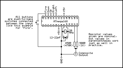
Even though it was always recommended as an excellent game for beginners to write, I don't believe I've ever written a Tetris clone before. Its simple block graphics makes it an ideal candidate for this system, and it always helps to work on a game that's fun to play. Armed with a Game Boy and a stopwatch I attempted to recreate a moderately faithful version of what is probably the most popular rendition of the game.
I think the result plays pretty well, but don't take my word for it — if you have an ATmega168 lying around, you can download the source and binaries here.
USB joypads and text on your TV courtesy of an ATmega168
Saturday, 14th November 2009
Nearly a month since my last update - my, how time flies when you're having fun (or a heavy workload).
I ended up building myself a cheap and cheerful SI Prog programmer for AVR development. After installing the development tools, scanning through the documentation and writing the microcontroller equivalent of Hello, World (flashing an LED on and off) I needed to find a suitable project. The first one was getting to grips with V-USB, a software USB implementation for AVRs. All you need for this are a couple of I/O pins, a few configuration file changes to set your USB device's vendor ID, product ID and device class, and a few lines of C code to actually implement your device. I attached six tactile switches to an ATmega168 and made the most uncomfortable USB joypad I've ever used. I managed two levels of Sonic the Hedgehog before my thumbs admitted defeat, but it's nice to know that building USB devices is very easy with an AVR.
#include <avr/io.h>
#include <avr/interrupt.h>
#include <avr/wdt.h>
#include <util/delay.h>
#include <avr/sleep.h>

#include "usbdrv.h"

/* Joystick port bits */
#define JOY_1     (1<<0)
#define JOY_2     (1<<1)
#define JOY_UP    (1<<2)
#define JOY_DOWN  (1<<3)
#define JOY_LEFT  (1<<4)
#define JOY_RIGHT (1<<5)

/* USB HID report descriptor */
PROGMEM char usbHidReportDescriptor[USB_CFG_HID_REPORT_DESCRIPTOR_LENGTH] = {
    0x05, 0x01,        // USAGE_PAGE (Generic Desktop)
    0x09, 0x05,        // USAGE (Game Pad)
    0xa1, 0x01,        // COLLECTION (Application)
    0x09, 0x01,        //   USAGE (Pointer)
    0xa1, 0x00,        //   COLLECTION (Physical)
    0x09, 0x30,        //     USAGE (X)
    0x09, 0x31,        //     USAGE (Y)
    0x15, 0x00,        //   LOGICAL_MINIMUM (0)
    0x26, 0xff, 0x00,  //     LOGICAL_MAXIMUM (255)
    0x75, 0x08,        //   REPORT_SIZE (8)
    0x95, 0x02,        //   REPORT_COUNT (2)
    0x81, 0x02,        //   INPUT (Data,Var,Abs)
    0xc0,              // END_COLLECTION
    0x05, 0x09,        // USAGE_PAGE (Button)
    0x19, 0x01,        //   USAGE_MINIMUM (Button 1)
    0x29, 0x02,        //   USAGE_MAXIMUM (Button 2)
    0x15, 0x00,        //   LOGICAL_MINIMUM (0)
    0x25, 0x01,        //   LOGICAL_MAXIMUM (1)
    0x75, 0x01,        // REPORT_SIZE (1)
    0x95, 0x08,        // REPORT_COUNT (8)
    0x81, 0x02,        // INPUT (Data,Var,Abs)
    0xc0               // END_COLLECTION
};

static uchar reportBuffer[3];    /* Buffer for HID reports */
static uchar idleRate;           /* 4 ms units */

uchar usbFunctionSetup(uchar data[8]) {
    usbRequest_t  *rq = (void*)data;
    usbMsgPtr = reportBuffer;
    if ((rq->bmRequestType & USBRQ_TYPE_MASK) == USBRQ_TYPE_CLASS) {
        switch (rq->bRequest) {
            case USBRQ_HID_GET_REPORT:
                return sizeof(reportBuffer);
            case USBRQ_HID_GET_IDLE:
                usbMsgPtr = &idleRate;
                return 1;
            case USBRQ_HID_SET_IDLE:
                idleRate = rq->wValue.bytes[1];
                break;
        }
    }
    return 0;
}

ISR(TIMER0_OVF_vect) {

    /* Fetch input */
    uchar input = ~PINC;

    /* X-axis */
    switch (input & (JOY_LEFT | JOY_RIGHT)) {
        case JOY_LEFT:
            reportBuffer[0] = 0;
            break;
        case JOY_RIGHT:
            reportBuffer[0] = 255;
            break;
        default:
            reportBuffer[0] = 128;
            break;
    }

    /* Y-axis */
    switch (input & (JOY_UP | JOY_DOWN)) {
        case JOY_UP:
            reportBuffer[1] = 0;
            break;
        case JOY_DOWN:
            reportBuffer[1] = 255;
            break;
        default:
            reportBuffer[1] = 128;
            break;
    }

    /* Buttons */
    reportBuffer[2] = input & (JOY_1 | JOY_2);

    usbPoll();
    usbSetInterrupt(reportBuffer, sizeof(reportBuffer));
};

int main(void) {

    usbInit();              /* Initialise USB. */

    PORTC = 0b00111111;     /* Pull high PORTC0..PORTC5 */

    TCCR0B = 0b00000101;    /* CS2..CS0 = 101:  prescaler = /1024 */
    TIMSK0 |= (1 << TOIE0); /* Enable timer 0 overflow interrupt. */
    sei();                  /* Enable global interrupts. */

    for (;;) {
        /* Infinite loop */
    }
}
I should only really call usbSetInterrupt when a button or axis has changed, rather than every loop, but the above code works as is.
One thing that always bothers me when it comes to electronic projects is the difficulty of providing text output. LCDs are generally quite expensive and low resolution, and typically require a great many pins to drive them. Video display processor chips are difficult to find, and appear to require quite complex external circuitry (the best thing I've found thus far are some TMS9918 chips being sold as spares for MSX computers). Having briefly experimented with generating PAL video signals in software before, I thought I'd try the two-resistor approach to getting PAL video output on an ATmega168.
I had a hunt around and found AVGA, which is close to what I wanted - video output from an AVR using cheap hardware. However, it outputs RGB directly, and I don't own a TV or RGB converter so couldn't use that - all I have is a VGA box (accepting composite or S-Video input) and a TV capture card (also only accepting composite or S-Video input). AVGA does work with VGA monitors, but I'd like to keep the hardware interface simple - just two resistors, ideally.
In the end, I ended up writing my own library. It currently has the following specifications:
- 32×16 characters: 512 bytes (half of the total SRAM on the ATmega168) are used to store the text buffer.
- Full 256 characters at a resolution of 6×8 pixels each.
- Total screen resolution: 192×128.
The library is interrupt-driven, and uses the sixteen-bit TIMER1 to schedule events. This means that the AVR is only busy generating video signals when it absolutely has to, leaving some CPU time to the user program. When outputting at full quality, the AVR appears to be capable of running user code at 3.3 MIPS, but by skipping alternate scanlines (each scanline is scanned twice anyway, so this mainly just makes the display appear darker) the AVR appears to be running user code at 9.9 MIPS. (I say "appears" as my calculation has been to execute a busy loop that would normally take one second on the AVR running at its normal 20 MIPS then seeing how long it takes with the video output driver enabled).
The above video demonstrates some of the currently rather limited features of the library. The text console handles a subset of the BBC Micro VDU commands - I'd like to support as many of its features as possible. The code behind the BASIC-like part of the demo is simply written like this:
#include "tvtext/tvtext.h"

void type_string_P(const char* s) {
    char c;
    while ((c = pgm_read_byte(s++))) {
        tvtext_putc(c);
        delay_ms(100);
    }
}

int main(void) {

    tvtext_init();

    tvtext_clear();
    tvtext_puts_P(PSTR("AVR Computer 1K\r\n\nATmega 168\r\n\nBASIC\r\n\n>"));
    delay_ms(2000);
    type_string_P(PSTR("10 PRINT \"AVR Rules! \";\r\n"));
    tvtext_putc('>');
    delay_ms(500);
    type_string_P(PSTR("20 GOTO 10\r\n"));
    tvtext_putc('>');
    delay_ms(500);
    type_string_P(PSTR("RUN"));
    delay_ms(1000);
    tvtext_puts_P(PSTR("\r\n"));

    for (int i = 0; i <= 200; ++i) {
        tvtext_puts_P(PSTR("AVR Rules! "));
        delay_ms(20);
    }

    tvtext_puts_P(PSTR("\r\nEscape at line 10\r\n>"));
    delay_ms(1000);
    type_string_P(PSTR("CHAIN \"DEMO\""));
    delay_ms(1000);

    // ...

}
All of the high-level console code - text output, viewport scrolling, cursor positioning &c - has been written in C, so should be relatively easy to be customised. The output driver itself has been written in assembly as timing is critically important.
With a few more features and a bit of tidying up I hope that people would find this a useful library. I'd certainly like to get a blinking cursor working within the driver, and if I add support for a reduced 128-character version I could save quite a bit of ROM space and add support for "coloured" - inverted, that is - text. NTSC support would also be quite useful.
64-bit IThumbnailProvider, BBC BASIC matrices and clocks
Friday, 16th October 2009
Work commitments have left me with little time to pursue my own projects of late, hence the lack of updates.
A chap named Jeremy contacted me with problems relating to the IThumbnailProvider code I'd posted here before. We narrowed it down to a 64-bit issue, demonstrated by the fact that the thumbnails appeared in the file open dialog of a 32-bit application, but not in Explorer. Not having a 64-bit version of Windows to tinker with, I was unable to help, but he found the solution was to register the assembly using the 64-bit version of regasm. You can read more about his experiences on his blog.
I had made a mistake in the BBC BASIC (Z80) for TI-83+ documentation, describing the old coordinate system in the graphics documentation rather than the current one (which is more closely aligned to other versions of BBC BASIC). I have uploaded a new version of the documentation to ticalc.org. This build also includes some basic matrix operations via the MAT statement. This statement is rather incomplete, but I've run out of ROM space (not to mention time) to implement it fully. Still, the bits that are there are quite useful, and a half-arsed implementation is better than no implementation... right?
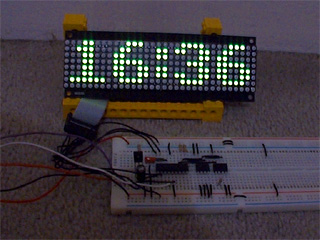
On a whim, I purchased a 32×8 LED display on eBay which I've (very) slowly been turning into a remote-controlled clock. A Sony-compatible remote control is used to type in the time, after which you can cycle through different styles with the channel up/down buttons and change the brightness with the volume and mute buttons. I'm using a 4MHz PIC16F84 to drive the display, with a DS1307 responsible for time-keeping and a 32KB 24LC256 to store the font data and text strings.
As well as dates and times, I thought a thermometer might be a useful addition so I put together an order for a DS18B20. It's silly to just order one thing, so I bulked up the order with one of the snazzy new PICAXE-20X2 chips (yes, they run a BASIC interpreter but the new 64MHz clock speed is certainly impressive). I find PICAXE microcontrollers invaluable for prototyping, being so very easy to use!
In an attempt to broaden my horizons, I also purchased two AVRs, as I have zero experience with these popular chips. I went for the two ends of the scale as offered by the supplier - an ATmega168 and an ATtiny13. Having lost a battle with PayPal's cart (it kept forgetting old items as I added new ones) I neglected to purchase a D-sub hood so I'll be waiting until I can go and buy one before I start assembling a programmer. I was intending on going for the simple SI Prog, but if anyone has any suggestions for variations I'd be interested in hearing them!
Taking advantage of interlacing for 3D
Friday, 7th August 2009
To achieve smooth, glitch-free 3D in an ideal world, one would like to be able to alternate between left and right eye views every time the monitor refreshes. You could then use the monitor's vertical synchronisation pulse to alternate which eye shutter is currently open.
Relying on software is not so bad if you can guarantee that you will be able to keep up with the video hardware and output alternating frames without dropping any. This is pretty much impossible with today's complex operating systems running any number of background tasks that could interfere with your render loop at any moment.
Fortunately, video cards already have a mode that is guaranteed to output a different image every frame - interlaced scan. Rather than send each scanline (row) of the image every frame ("progressive scan"), it alternates between sending every even-numbered scanline and every odd-numbered scanline. This halves the vertical resolution, but allows you to double the refresh rate using the same amount of bandwidth.

We can take advantage of this scan mode to encode the left and right views into a single image. The view for the left eye is stored in the even-numbered scanlines and the view for the right eye is stored in the odd-numbered scanlines, as in the image above. When displayed on a monitor using interlaced scan, it appears as the following:
As the video card takes care of alternating which set of scanlines (or field) is displayed, the result is that the left and right views alternate perfectly in time with the monitor's refresh rate.
To test this, I've attached a counter IC to the vertical synchronisation pulse of a VGA monitor. The low bit of the counter toggles every time the screen refreshes, and this is used to select which eye shutter is open on the 3D glasses. The glasses are driven using the serial port adaptor described in the previous post.
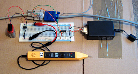
The result is perfectly stable 3D images. The circuit does not know which field, and hence which eye's view, is visible at any time - it just alternates left and right, which means that there is a 50% chance that the left and right views are flipped. This can be fixed by switching the circuit off then on again to try and resynchronise, but a better solution would be to add a switch to toggle the uncovered eye manually and to fix the synchronisation. As this would only need to be done once per session this isn't much of an issue! An alternative fix would be to add a switch to switch the left and right views in software.
The logic probe in the above photo is an integral part of the design - at least, I assume it is, as if I remove it the circuit doesn't work correctly! I assume there's a noise issue that's interfering with the circuit (none of the unused inputs on the counter chip are tied low) and the logic probe contains some noise suppression circuitry of its own.
The only real fly in the ointment here is video driver support for interlaced scan modes. My video card only supports 1920×1080 at 30i, 29i and 25i, and only if the primary monitor is an LCD. I can work around the problem by cloning the primary LCD to the CRT and setting both to 1920×1080 at 30i, but my LCD displays a warning message and makes a distressing noise and 30i, whilst faithful to the Master System's 30fps 3D, is unpleasantly flickery. It would be wonderful if I could drop the resolution down a bit and switch to 60i, but I can't see a way to do that with ATi's drivers.
3D LCD Shutter Glasses Experimentation
Wednesday, 5th August 2009
The Sega Master System supported 3D LCD shutter glasses to provide a more immersive (if somewhat flickery) playing experience. Having caught wind of an eBay member selling compatible glasses for $9 and being rather interested in stereoscopy I decided to experiment a little for myself.
The glasses are pretty simple; they consist of two LCD panels that can be "switched on" to block light from passing through to each eye. A 3.5mm stereo jack plug provides the electrical connection.
To display the 3D image you alternate between showing the image for the left eye and the right eye on the monitor, uncovering the corresponding eye immediately before the image appears on the monitor. This effectively halves the refresh rate (and results in fairly noticeable flicker when run at the standard NTSC 60Hz) and prevents the 3D glasses from working with displays that respond too slowly (eg LCD panels). I've had to dig out my old CRT monitor for this project. Even if my LCD did refresh quickly enough, its polarisation is perpendicular to the polarisation of the shutter glasses, meaning that no light can pass from the LCD through the glasses even when both eye LCD panels are switched off.
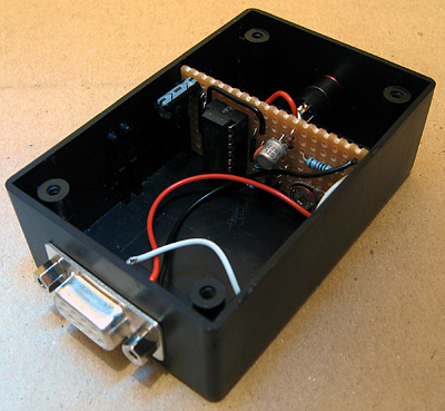
The adaptor I'm using is based on this circuit (I'm using the second variation with the variable resistor to fine-tune the driving frequency). The LCD panels require an AC voltage, and using a EOR gate as an oscillator allows the whole device to be constructed out of a single IC with a handful of external components. More importantly, being based on an existing and public design allows me to ensure that any work I do should be compatible with adaptors other people have built.
The DTR pin on the serial port supplies power to the circuit and the RTS pin is used to choose which LCD panel is switched on to cover an eye.
Test pattern seen through glasses
The above image displays a test pattern viewed through the glasses. The software alternates between clearing the screen to red with the left eye shutter open and clearing the screen to cyan with the right eye shutter open. The colours were deliberately chosen to match the colours of the common anaglyph glasses. As the colours are alternated very quickly (in the interests of avoiding a headache I used a refresh rate of 120Hz) the screen appears a light grey colour to the naked eye.
Most LCD shutter glasses appear to use some form of feedback from the video signal to synchronise the alternating of eyes. On a PC they could alternate every time the vsync signal appeared on the VGA port, on a TV they could open the correct eye shutter depending on the current field of the interlaced image that was being displayed. The Sega Master System's video chip can generate an interrupt when entering the vblank period which you can use to prepare the next frame and update the glasses. An adaptor connected to the PC's serial port has no such luck - I have not yet found a way to reliably synchronise the glasses to the refresh rate.
Poor synchronisation (and even worse photography) results in images like the above, as seen through the left shutter. As the LCD shutters have been updated too late, some of the display intended for the right eye is seen through the left eye at the top of the display - the cyan band in this case.
So far, the best result I've had is to use Direct3DEx's DeviceEx, which provides a handy WaitForVBlank method. Less handy is the Vista requirement, as is the slight delay between returning from this function and updating the serial port, resulting in a flickering band near the top of the display as per the previous photograph. For the best results I need to set the presentation interval to "immediate", which compounds the issue with occasional tearing caused by the delay between WaitForVBlank returning and calling Present.
Switching the presentation interval back to "1" (tying the refresh rate of the render loop to that of the monitor) results in complete frames (no tearing or bands of the wrong colour/image), but the additional delay before presenting the next frame puts updating the LCD glasses out of sync by one frame. As the uncovered eye should alternate between subsequent frames one can simply uncover the "opposite" eye to uncover the correct image, but any dropped frames throw this out of sync and you get the occasional "inside out" view when the wrong eye is uncovered. Any background tasks on the PC kicking in could potentially cause a dropped frame. This is one reason that a VGA pass-through adaptor that automatically alternates the uncovered eye every frame wouldn't work, as it would get thrown out of sync by these dropped frames.

A demo compatible with the Sega 3D glasses, showing the images for each eye as stereo pair
The advantage of using an existing adaptor design makes me reluctant to pursue solutions that involve additional hardware to fix the problem. One possible solution I can think of would be an additional pass-through box that contains a simple latch that is clocked by the VGA vsync signal between the serial port and the glasses adaptor. You could then set the state of the glasses immediately before calling Present, safe in the knowledge that your signal will only get through to the adaptor box perfectly synchronised with the CRT's vertical refresh, assuming the CRT doesn't enter vblank between updating the serial port and calling Present. Not having to manually synchronise to vsync in software would remove the need for the Vista-only Direct3DEx too.
Remote controlling Windows the Sony way
Wednesday, 27th May 2009
It's been a while since I last posted, and unfortunately this post is to do with Sony remote controls again. 
This time I'm attempting to use Sony (or compatible) remote controls to control software running on a Windows PC. I've recently been watching more films in PowerDVD, and some of the keyboard shortcuts (eg Ctrl+P for the menu) are a little difficult to hit in the dark and from a distance. I have a ready supply of universal remote controls as well as the PlayStation 2 DVD remote control, all of which work with the SIRCS protocol.
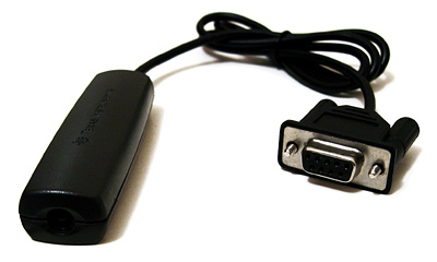
Serial port infra-red receiver built into an old TI GraphLink cable
First up is the required hardware. This involves an infrared demodulator connected to a free serial port. I chose the serial port as .NET provides a way to handle pin change events and you do not need administrator rights to access it (as per the parallel port). I also had a broken Texas Instruments GraphLink cable that could be ripped apart to act as a case.
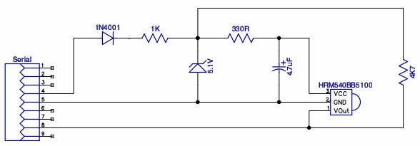
Infra-red receiver module schematic
The circuit is pretty simple. Pin 4 (DTR) and 5 (GND) from the serial port form the power supply. DTR can be set to either +12V or -12V, so a rectifier diode is used to keep the input voltage above 0V. Following that is a reverse-biased zener diode and resistor to regulate the voltage below 5.1V. Finally, the output pin of the infra-red demodulator is connected to the input pin 8 (CTS) of the serial port.
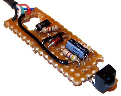
Infra-red receiver module assembled on stripboard
The software handles the SerialPort.PinChanged event to time the length of input pulses. Once it detects a start bit (2.4mS) it starts decoding the rest of the command. When it's finished receiving a command it fires an event of its own, which the main software can react to.
using System;
using System.Diagnostics;
using System.IO.Ports;

namespace BeeDevelopment.Sircs {

    /// <summary>
    /// Represents a command sent by a SIRCS remote control.
    /// </summary>
    public struct SircsCommand : IEquatable<SircsCommand> {

        #region Properties

        private byte command;
        /// <summary>
        /// Gets or sets the command value.
        /// </summary>
        public byte Command {
            get { return this.command; }
            set { this.command = value; }
        }

        private short device;
        /// <summary>
        /// Gets or sets the device identifier.
        /// </summary>
        public short Device {
            get { return this.device; }
            set { this.device = value; }
        }

        private int length;
        /// <summary>
        /// Gets or sets the length of the command in bits.
        /// </summary>
        public int Length {
            get { return this.length; }
            set { this.length = value; }
        }

        #endregion

        #region Construction

        /// <summary>
        /// Creates an instance of a <see cref="SircsCommand"/> structure.
        /// </summary>
        /// <param name="command">The command value.</param>
        /// <param name="device">The device identifier.</param>
        /// <param name="length">The length of the command in bits.</param>
        public SircsCommand(byte command, short device, int length) {
            this.command = command;
            this.device = device;
            this.length = length;
        }

        #endregion

        #region Methods

        /// <summary>
        /// Converts the <see cref="SircsCommand"/> into a string.
        /// </summary>
        /// <returns>A string representation of the <see cref="SircsCommand"/>.</returns>
        public override string ToString() {
            return string.Format("Command={0:X2}, Device={1:X4}, Length={2}", this.command, this.device, this.length);
        }

        /// <summary>
        /// Returns the hash code for this instance.
        /// </summary>
        /// <returns>The hash code for this instance.</returns>
        public override int GetHashCode() {
            return this.command ^ this.device ^ this.length;
        }

        /// <summary>
        /// Returns a value indicating whether this instance is equal to another <see cref="SircsCommand"/> instance.
        /// </summary>
        /// <param name="other">The instance to compare to this one for equality.</param>
        /// <returns>True if the instances are equal, false otherwise.</returns>
        public bool Equals(SircsCommand other) {
            return this.command == other.command && this.device == other.device && this.length == other.length;
        }

        /// <summary>
        /// Returns a value indicating whether this instance is equal to another <see cref="SircsCommand"/> instance.
        /// </summary>
        /// <param name="other">The instance to compare to this one for equality.</param>
        /// <returns>True if the instances are equal, false otherwise.</returns>
        public override bool Equals(object other) {
            return other != null && other is SircsCommand && ((SircsCommand)other).Equals(this);
        }

        #endregion

        #region Operators

        public static bool operator ==(SircsCommand a, SircsCommand b) { return a.Equals(b); }
        public static bool operator !=(SircsCommand a, SircsCommand b) { return !a.Equals(b); }

        #endregion

    }

    #region Events

    /// <summary>
    /// Represents the method that will handle the <c>SircsCommandReceived</c> event.
    /// </summary>
    /// <param name="sender">The object that fired the event.</param>
    /// <param name="e">Information about the event.</param>
    public delegate void SircsCommandReceivedEventHandler(object sender, SircsCommandReceivedEventArgs e);

    /// <summary>
    /// Provides data for the <c>SircsReceived.SircsCommandReceived</c> event.
    /// </summary>
    public class SircsCommandReceivedEventArgs : EventArgs {

        #region Properties

        /// <summary>
        /// Gets the <see cref="SircsCommand"/> that was received.
        /// </summary>
        public SircsCommand Command { get; private set; }

        /// <summary>
        /// Gets the number of times that the incoming command has been repeated when held.
        /// </summary>
        public int Repeat { get; private set; }

        #endregion

        #region Construction

        /// <summary>
        /// Creates a <see cref="SircsCommandReceivedEventArgs"/> instance.
        /// </summary>
        /// <param name="command">The <see cref="SircsCommand"/> that was recieved.</param>
        /// <param name="repeat">The number of times that the incoming command has been repeated when held.</param>
        public SircsCommandReceivedEventArgs(SircsCommand command, int repeat) {
            this.Command = command;
            this.Repeat = repeat;
        }

        #endregion

        #region Methods

        /// <summary>
        /// Converts the <see cref="SircsCommandReceivedEventArgs"/> into a string.
        /// </summary>
        /// <returns>A string representation of the <see cref="SircsCommandReceivedEventArgs"/>.</returns>
        public override string ToString() {
            return string.Format("{0}, Repeat={1}", this.Command, this.Repeat);
        }

        #endregion
    }

    #endregion

    /// <summary>
    /// Provides a way to receive SIRCS commands from a simple receiver attached to a serial port.
    /// </summary>
    public class SircsReceiver : IDisposable {

        #region Constants

        /// <summary>
        /// The minimum time length for a start bit (nominally 2.4ms).
        /// </summary>
        private const double StartBitMinLength = 2.0E-3;

        /// <summary>
        /// Threshold time length between a "low" (0.6ms) and a "high" (1.2ms) bit.
        /// </summary>
        private const double DataBitLengthThreshold = 0.9E-3;

        /// <summary>
        /// The maximum time length between data bits. If this is exceeded, any data command transfer is cancelled.
        /// </summary>
        private const double IntraBitMaxLength = 0.8E-3;

        /// <summary>
        /// The maximum time length between repeating commands. Commands are supposed to repeat every 45ms.
        /// </summary>
        private const double RepeatCommandMaxLength = 120.0E-3;

        #endregion

        #region Private Fields

        /// <summary>
        /// The <see cref="SerialPort"/> that the receiver is connected to.
        /// </summary>
        private SerialPort Port = null;

        /// <summary>
        /// The last time that the pin state changed in ticks.
        /// </summary>
        private long LastPinChangedTime = 0;

        /// <summary>
        /// A <see cref="Stopwatch"/> instance used to time incoming bits.
        /// </summary>
        private Stopwatch BitTimer = null;

        /// <summary>
        /// Set to <c>true</c> when receiving a command, <c>false</c> otherwise.
        /// </summary>
        private bool ReceivingCommand = false;

        /// <summary>
        /// Counts the number of bits currently received.
        /// </summary>
        private int BitsReceived = 0;

        /// <summary>
        /// Stores the command as it gets built up.
        /// </summary>
        private uint Command = 0;

        /// <summary>
        /// Stores the last received command.
        /// </summary>
        private SircsCommand LastCommand = default(SircsCommand);

        /// <summary>
        /// Stores the number of times the received command has been repeated.
        /// </summary>
        private int LastCommandRepeatCount = 0;

        /// <summary>
        /// A <see cref="Stopwatch"/> instance used to time repeating commands.
        /// </summary>
        private Stopwatch RepeatTimer = null;

        #endregion

        #region Construction/Destruction

        /// <summary>
        /// Creates an instance of a <see cref="SircsReceiver"/> from a serial port name.
        /// </summary>
        /// <param name="portName">The name of the serial port the receiver is connected to.</param>
        public SircsReceiver(string portName) {

            // Set up the serial port.
            this.Port = new SerialPort(portName);
            this.Port.PinChanged += new SerialPinChangedEventHandler(PinChanged);

            // Open the port for access.
            this.Port.Open();
            this.Port.DtrEnable = true;
            this.Port.RtsEnable = true;

            // Get the timers running.
            this.BitTimer = new Stopwatch();
            this.BitTimer.Start();
            this.RepeatTimer = new Stopwatch();
            this.RepeatTimer.Start();
        }

        /// <summary>
        /// Releases the resources used by this <see cref="SircsReceiver"/> instance.
        /// </summary>
        public void Dispose() {
            if (this.Port != null) {
                this.Port.PinChanged -= new SerialPinChangedEventHandler(PinChanged);
                this.Port.Dispose();
                this.Port = null;
            }
        }

        ~SircsReceiver() {
            this.Dispose();
        }

        #endregion

        #region Events

        /// <summary>
        /// An event that is fired when a <see cref="SircsCommand"/> is received.
        /// </summary>
        public event SircsCommandReceivedEventHandler SircsCommandReceived;

        /// <summary>
        /// A method that is invoked when a <see cref="SircsCommand"/> is received.
        /// </summary>
        /// <param name="e"></param>
        protected virtual void OnSircsCommandReceived(SircsCommandReceivedEventArgs e) {
            if (this.SircsCommandReceived != null) this.SircsCommandReceived(this, e);
        }

        #endregion

        #region SIRCS protocol handling

        void PinChanged(object sender, SerialPinChangedEventArgs e) {

            // Respond to changes on the CTS pin.
            if (e.EventType == SerialPinChange.CtsChanged) {

                // Quickly grab the current time and current CTS level.
                long CurrentPinChangedTime = this.BitTimer.ElapsedTicks;
                bool CurrentLevel = this.Port.CtsHolding;

                // Calculate the time elapsed.
                long DeltaTime = CurrentPinChangedTime - this.LastPinChangedTime;
                double SecondsElapsed = (double)DeltaTime / (double)Stopwatch.Frequency;
                this.LastPinChangedTime = CurrentPinChangedTime;

                if (CurrentLevel) { // If the current signal level is high, we may assume that we've just timed a low pulse.

                    // Have we received a start bit?
                    if (SecondsElapsed > SircsReceiver.StartBitMinLength) {
                        this.ReceivingCommand = true;
                        this.BitsReceived = 0;
                        this.Command = 0;
                    } else if (this.ReceivingCommand) {
                        // Process incoming bit.
                        this.Command >>= 1;
                        if (SecondsElapsed > SircsReceiver.DataBitLengthThreshold) {
                            this.Command |= unchecked((uint)(1 << 31));
                        }

                        // Have we received enough bits?
                        switch (++this.BitsReceived) {
                            case 12:
                            case 15:
                            case 20:
                                // We've received enough bits to handle the input as a received command.
                                // Check to see if there's any more data forthcoming.
                                long EndTime = CurrentPinChangedTime + (long)(Stopwatch.Frequency * SircsReceiver.IntraBitMaxLength);
                                while (BitTimer.ElapsedTicks < EndTime) {
                                    if (!(CurrentLevel = this.Port.CtsHolding)) break;
                                }
                                // The input is still high - there's no more data coming in; we've received a command.
                                if (CurrentLevel) {
                                    // Construct a struct to hold information about the recieved data.
                                    SircsCommand ReceivedCommand = new SircsCommand(
                                        (byte)((this.Command >> (32 - this.BitsReceived)) & 0x7F),
                                        (short)(this.Command >> ((32 + 7) - this.BitsReceived)),
                                        this.BitsReceived
                                    );

                                    // Reset the timer.
                                    this.ReceivingCommand = false;
                                    this.BitTimer.Reset();
                                    this.BitTimer.Start();
                                    this.LastPinChangedTime = 0;

                                    // Calculate the repeat count.

                                    // Quickly grab the current time and current CTS level.
                                    long RepeatTimeTicks = this.RepeatTimer.ElapsedTicks;
                                    this.RepeatTimer.Reset();
                                    this.RepeatTimer.Start();

                                    // Calculate the repeat time elapsed.
                                    double RepeatTimeSeconds = (double)RepeatTimeTicks / (double)Stopwatch.Frequency;

                                    // Is the command repeating?
                                    if (ReceivedCommand == this.LastCommand && RepeatTimeSeconds < SircsReceiver.RepeatCommandMaxLength) {
                                        ++this.LastCommandRepeatCount;
                                    } else {
                                        this.LastCommandRepeatCount = 1;
                                        this.LastCommand = ReceivedCommand;
                                    }

                                    // Fire the event.
                                    this.OnSircsCommandReceived(new SircsCommandReceivedEventArgs(ReceivedCommand, this.LastCommandRepeatCount));
                                }
                                break;
                        }
                    }
                } else { // If the current signal level is low, we may assume that we've just timed a high pulse.
                    // If a high pulse is too long, cancel any incoming commands.
                    if (SecondsElapsed > SircsReceiver.IntraBitMaxLength) {
                        this.ReceivingCommand = false;
                        this.BitTimer.Reset();
                        this.BitTimer.Start();
                        this.LastPinChangedTime = 0;
                    }
                }
            }
        }

        #endregion

    }
}
Currently, the software reacts to input events by running through a list of scripts, passing the command ID, device ID and command length (in bits) to each until one of them returns zero (ie, success) to indicate that it has processed the button.
Scripts list
The advantage to this method is that the end-user could customise the behaviour of the software to their own liking very easily. For example, here's the PowerDVD.js file from above, which allows me to control PowerDVD from a PlayStation 2 DVD remote control:
// Table of commands.
var Commands = [
    { Command : 0x00, Device : 0x093A, Length : 20, Shortcut : '1' },         // 1
    { Command : 0x01, Device : 0x093A, Length : 20, Shortcut : '2' },         // 2
    { Command : 0x02, Device : 0x093A, Length : 20, Shortcut : '3' },         // 3
    { Command : 0x03, Device : 0x093A, Length : 20, Shortcut : '4' },         // 4
    { Command : 0x04, Device : 0x093A, Length : 20, Shortcut : '5' },         // 5
    { Command : 0x05, Device : 0x093A, Length : 20, Shortcut : '6' },         // 6
    { Command : 0x06, Device : 0x093A, Length : 20, Shortcut : '7' },         // 7
    { Command : 0x07, Device : 0x093A, Length : 20, Shortcut : '8' },         // 8
    { Command : 0x08, Device : 0x093A, Length : 20, Shortcut : '9' },         // 9
    { Command : 0x09, Device : 0x093A, Length : 20, Shortcut : '0' },         // 0
    { Command : 0x0B, Device : 0x093A, Length : 20, Shortcut : '{ENTER}' },   // Enter
    { Command : 0x0E, Device : 0x093A, Length : 20, Shortcut : '{ESC}' },     // Return
    { Command : 0x1A, Device : 0x093A, Length : 20, Shortcut : 'lt' },        // Title
    { Command : 0x2A, Device : 0x093A, Length : 20, Shortcut : 'x' },         // A<->B
    { Command : 0x28, Device : 0x093A, Length : 20, Shortcut : 'd' },         // Time
    { Command : 0x2C, Device : 0x093A, Length : 20, Shortcut : '^r' },        // Repeat
    { Command : 0x30, Device : 0x093A, Length : 20, Shortcut : 'p' },         // Previous
    { Command : 0x31, Device : 0x093A, Length : 20, Shortcut : 'n' },         // Next
    { Command : 0x32, Device : 0x093A, Length : 20, Shortcut : '{ENTER}' },   // Play
    { Command : 0x33, Device : 0x093A, Length : 20, Shortcut : 'b' },         // Scan <<
    { Command : 0x34, Device : 0x093A, Length : 20, Shortcut : 'f' },         // Scan >>
    { Command : 0x38, Device : 0x093A, Length : 20, Shortcut : 's' },         // Stop
    { Command : 0x39, Device : 0x093A, Length : 20, Shortcut : ' ' },         // Pause
    { Command : 0x54, Device : 0x093A, Length : 20, Shortcut : 'z' },         // Display
    { Command : 0x60, Device : 0x093A, Length : 20, Shortcut : '^b' },        // Slow <<
    { Command : 0x61, Device : 0x093A, Length : 20, Shortcut : 't' },         // Slow >>
    { Command : 0x63, Device : 0x093A, Length : 20, Shortcut : 'u' },         // Subtitle
    { Command : 0x64, Device : 0x093A, Length : 20, Shortcut : 'h' },         // Audio
    { Command : 0x65, Device : 0x093A, Length : 20, Shortcut : 'a' },         // Angle
    { Command : 0x79, Device : 0x093A, Length : 20, Shortcut : '{UP}' },      // Up
    { Command : 0x7A, Device : 0x093A, Length : 20, Shortcut : '{DOWN}' },    // Down
    { Command : 0x7B, Device : 0x093A, Length : 20, Shortcut : '{LEFT}' },    // Left
    { Command : 0x7C, Device : 0x093A, Length : 20, Shortcut : '{RIGHT}' },   // Right
];

// Search for the matching command.
var Command = null;
for (var enumerator = new Enumerator(Commands); !enumerator.atEnd(); enumerator.moveNext()) {
    var TestCommand = enumerator.item();
    if (TestCommand.Command == WScript.Arguments(1) && TestCommand.Device == WScript.Arguments(2) && TestCommand.Length == WScript.Arguments(3)) {
        Command = TestCommand;
        break;
    }
}

// No command.
if (!Command) WScript.Quit(1);

// Find the PowerDVD process ID.
var PowerDvdId = null;
var WmiService = GetObject('winmgmts://./root/cimv2');
var Processes = WmiService.ExecQuery('Select ProcessId From Win32_Process Where Name="PowerDVD.exe"');
for (var enumerator = new Enumerator(Processes); !enumerator.atEnd(); enumerator.moveNext()) {
    PowerDvdId = enumerator.item().ProcessId;
    break;
}

// If we haven't found the process ID, quit with an error.
if (!PowerDvdId) WScript.Quit(1);

// Activate the PowerDVD instance.
var WshShell = new ActiveXObject('WScript.Shell');
WshShell.AppActivate(PowerDvdId);

// Send the shortcut keys.
WshShell.SendKeys(Command.Shortcut);

WScript.Quit(0);
Unfortunately, this method has quite a lot of overhead. This becomes a problem when you consider that commands are repeated every 45ms. Currently I avoid the issue by not allowing any keys to repeat, but some keys - such as the volume keys - would need to repeat when held.
I'm unsure as the best path to take. One idea that has crossed my mind would be to set up each remote control you were going to use beforehand (though I suppose I could build up a database of remote controls and bundle them with the software). You could then set whether each key should repeat or not, and attach a meaningful string to each button. This would also allow for more protocols to be supported other than SIRCS, and you could set it up so that the Play button on a Sony remote control generated the string "play" and passed that to the script(s) as well as the Play button on a Panasonic or Toshiba remote control rather than juggling control codes.
Decoding SIRCS commands with a PIC16F84
Sunday, 1st March 2009
Some time ago I was working on a simple Z80-based computer. It has a PS/2 keyboard and mouse port for user input, and these are implemented using a large number of discrete parts - transistor drivers with all manner of supporting latches and buffers. The AT protocol (which the PS/2 keyboard and mouse inherit) is entirely implemented in software by the Z80.
On the one hand this design has a certain purity, but it ties the CPU up every time data is to be transferred. The keyboard sends data when it feels like it, so if you wished to perform some function based on a key press event you'd need to poll the port periodically, assuming that if communications time out there's no key waiting. All this hanging around does nothing good for performance.
As it turns out I found a PIC16F84 in an old school project over the weekend, so downloaded its datasheet and the MPLAB IDE and tried to puzzle it out.
The 16F84 is a pretty venerable microcontroller with a 1K flash memory for program code, 68 bytes of data RAM and 64 bytes of data EEPROM. It can run at up to 10MHz, and is based on a high-performance RISC CPU design. It has 13 digital I/O pins, each of which can be configured individually as either an input or an output. I'm well aware there are far better microcontrollers around these days, but this one was just sitting around doing nothing.
;if(img.style.backgroundImage){img.style.backgroundImage='url('+img.src+')';img.src=imgs[img.src.indexOf(imgs[1])<0?1:2]}else{img.style.backgroundImage='url('+img.src+')';img.src=imgs[2];};void(0);)
Above is the circuit I constructed to work with the 16F84. The HRM538BB5100 in the top-right is an infrared demodulator and amplifier module; it will output 5V until it receives a 38kHz infrared signal (such as the one emitted by most remote controls) at which point it outputs 0V. By timing the lengths of the IR pulses one could decode a remote control signal, and that's the aim of this project - decode a command from a Sony remote control and display it on the two 7-segment displays. The 10MHz crystal is probably overkill for this simple task, but it's the slowest I had available!
In fact, the 10MHz crystal works out quite neatly. Most instructions execute in one instruction cycle, which is four clock cycles. Four clock cycles at 10MHz is 400nS. The 16F84 has an internal timer that counts up after every instruction cycle and triggers an interrupt when it overflows from 255 back to 0; 400nS*256=102.4µs. If we call that 100µs (close enough for jazz) then it overflows 10 times every millisecond. The SIRCS protocol is based around multiples of 0.6ms, which makes this rate very easy to work with.
; ========================================================================== ;
; Pins:                                                                      ;
; RB0~RB6: Connected to A~G on the two seven-segment displays.               ;
; RB7:     Connected via a 220R resistor to cathode of the left display.     ;
;          Inverted and connected via a 220R resistor to right display's     ;
;          cathode.                                                          ;
; RA0:     Connected to the output of the HRM538BB5100.                      ;
; ========================================================================== ;

#include <p16F84.inc>

	list p=16F84

	__CONFIG   _CP_OFF & _WDT_OFF & _PWRTE_ON & _HS_OSC

; ========================================================================== ;
; Variables                                                                  ;
; ========================================================================== ;
	udata
IsrW       res 1 ; Temporary storage used to preserve state during the
IsrStatus  res 1 ; interrupt service routine.

Display    res 1 ; Value shown on 7-segment displays.

PulseTimer res 1 ; Counter to time the length of pulses.

BitCounter res 1 ; Number of bits being received.
Command    res 1 ; SIRCS command.

; ========================================================================== ;
; Reset                                                                      ;
; ========================================================================== ;
ResetVector code 0x0000
	goto Main

; ========================================================================== ;
; Interrupt Service Routine                                                  ;
; ========================================================================== ;
ISR code 0x0004

	; Preserve W and STATUS.
	movwf IsrW
	swapf STATUS,w
	movwf IsrStatus

	; Update value shown on two 7-segment displays.
	movfw Display
	btfsc PORTB,7
	swapf Display,w
	andlw h'F'
	call Get7SegBits
	btfss PORTB,7
	xorlw b'10000000'
	movwf PORTB

	; Increment pulse timer.
	incfsz PulseTimer,w
	movwf PulseTimer

	; Acknowledge timer interrupt.
	bcf INTCON,T0IF

	; Restore W and STATUS.
	swapf IsrStatus,w
	movwf STATUS
	swapf IsrW,f
	swapf IsrW,w
	retfie

; ========================================================================== ;
; Times the length of a "low" pulse.                                         ;
; ========================================================================== ;
; Out: W - Length of pulse.                                                  ;
; ========================================================================== ;
TimeLow
	clrf PulseTimer
TimeLow.Wait
	btfsc PORTA,0
	goto TimeLow.GoneHigh
	incfsz PulseTimer,w
	goto TimeLow.Wait
TimeLow.GoneHigh
	movfw PulseTimer
	return

; ========================================================================== ;
; Times the length of a "high" pulse.                                        ;
; ========================================================================== ;
; Out: W - Length of pulse.                                                  ;
; ========================================================================== ;
TimeHigh
	clrf PulseTimer
TimeHigh.Wait
	btfss PORTA,0
	goto TimeHigh.GoneLow
	incfsz PulseTimer,w
	goto TimeHigh.Wait
TimeHigh.GoneLow
	movfw PulseTimer
	return

; ========================================================================== ;
; Convert a hex nybble (0-F) into a format that can be displayed on a 7-seg  ;
; display.                                                                   ;
; ========================================================================== ;
; In: W. Out: W.                                                             ;
; ========================================================================== ;
Get7SegBits
	addwf PCL, f
	dt b'00111111' ; 0
	dt b'00000110' ; 1
	dt b'01011011' ; 2
	dt b'01001111' ; 3
	dt b'01100110' ; 4
	dt b'01101101' ; 5
	dt b'01111101' ; 6
	dt b'00000111' ; 7
	dt b'01111111' ; 8
	dt b'01101111' ; 9
	dt b'01110111' ; A
	dt b'01111100' ; b
	dt b'00111001' ; C
	dt b'01011110' ; d
	dt b'01111001' ; E
	dt b'01110001' ; F

; ========================================================================== ;
; Start of the main program.                                                 ;
; ========================================================================== ;
Main

	; Set PORTB to be an output.
	bsf STATUS,RP0
	clrw
	movwf TRISB
	bcf STATUS,RP0

	; Configure TMR0.
	bsf STATUS,RP0
	bcf OPTION_REG,T0CS ; Use internal instruction counter.
	bcf STATUS,RP0

	; Enable TMR0 interrupt.
	bsf INTCON,T0IE
	bsf INTCON,GIE

	clrf Display

; ========================================================================== ;
; Main program loop.                                                         ;
; ========================================================================== ;
Loop

WaitCommand
	; Loop around waiting for a low to indicate incoming data.
	btfsc PORTA,0
	goto WaitCommand

	; Start bit (2.4mS).
	call TimeLow
	; Check that it's > 2mS long.
	sublw d'20'
	btfsc STATUS,C
	goto WaitCommand ; w<=20

	; Reset the command variable and get ready to read 7 bits.
	clrf Command
	movlw d'7'
	movwf BitCounter

ReceiveBit
	; Time the pause; should be < 1mS.
	call TimeHigh
	sublw d'10'
	btfss STATUS,C
	goto WaitCommand

	; Time the input bit (0.6ms = low, 1.2ms = high).
	call TimeLow
	sublw d'9'
	; Shift into the command bit.
	rrf Command,f

	decfsz BitCounter,f
	goto ReceiveBit

	bsf STATUS,C
	rrf Command,f
	comf Command,f

	movfw Command
	movwf Display

	goto Loop

; ========================================================================== ;
; Fin.                                                                       ;
; ========================================================================== ;
	end
The final source code is above. I'm not sure how well-written it is, but it works; pointing a Sony remote control at the receiver and pressing a button changes the value shown on the seven-segment display. PICmicro assembly is going to get take a little getting used to; instructions are ordered "backwards" to the Intel order I'm used to (op source,destination instead of the more familiar op destination,source) and as far as I can tell literals default to being interpreted as hexadecimal as opposed to decimal.
With some luck I can now teach the 16F84 the AT protocol and replace a large number of parts on the Z80 computer project with a single IC. It does feel a little like cheating, though!
64KB RAM and a CHIP-8/SCHIP interpreter
Monday, 22nd September 2008
The only major hardware modification since last time is the addition of another 32KB SRAM.
;if(img.style.backgroundImage){img.style.backgroundImage='url('+img.src+')';img.src=imgs[img.src.indexOf(imgs[1])<0?1:2]}else{img.style.backgroundImage='url('+img.src+')';img.src=imgs[2];};void(0);)
This appears as two 16KB pages in the $4000..$7FFF slot. Currently only the first page is used for OS variables and scratch space, freeing up the upper 32KB entirely for BBC BASIC's use.
One other minor hardware addition is support for a dual-coloured LED on the control port. This LED will be used to signify file access - reads by a green LED and writes by a red LED. As such I haven't implemented a proper file system, but typing SAVE "FILE" or LOAD "FILE" at the prompt will transfer data between the Z80 RAM and a 24LC256 32KB EEPROM. The routines do not pay attention to any file name specified - the first two bytes on the EEPROM indicate the file size, and the rest of the EEPROM is the file. I think some sort of simplified version of FAT may work well, as the EEPROM has a natural page size of 64 bytes which could be used in place of clusters.
Adding the second 32KB SRAM required soldering wires to the underside of the stripboard, not something I'd recommend!
As I have not yet added any graphical commands to BBC BASIC, and as porting assembly programs to this hardware is going to be a bit of a pain until I decide on the way the OS is going to work, I decided to try and port Vinegar to the system. Vinegar is a CHIP-8 and SCHIP interpreter - CHIP-8 programs being simple bytecode and so relatively simple to interpret.
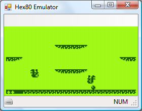
The code I had written was difficult to port, however, being inefficiently and messily written, so I ended up rewriting all of it apart from the sprite drawing routines. The TI-83+ LCD follows the usual trend of storing 8 horizontal pixels in each byte of video memory. The LCD I have stores 8 vertical pixels in each byte of video memory, which means that each 8×8 pixel block in memory needs to be rotated by 90° before being sent to the LCD hardware. This is understandably very slow, and not helped by the Z80 only running at 2MHz. To further complicate issues, games rely on two 60Hz timers, and I have no timing hardware. The current version of the interpreter has some bugs, but is good enough to run some SCHIP programs.
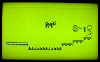
CHIP-8 programs are displayed squashed in the top-left hand corner, as they're designed to run in a 64×32 video mode unlike SCHIP's 128×64 (happily, the resolution of the LCD) - typically, the one thing I really did need to fix for the new hardware, the sprite code, is the only thing I copied over. In reality, CHIP-8 graphics would need to be scaled up to fit the screen. Working out a way of getting the system to operate at 10MHz would really be a welcome upgrade!
Times, backlights and off-page calls
Sunday, 14th September 2008
Dates, times and backlights
I'm using a DS1307 real-time clock to provide the computer with real-time date and time functions. It's a great little chip - all it needs is power, two lines for I2C communications, a 32768Hz crystal between two pins and a back-up battery to keep it ticking when main power is removed and it's happy. That accounts for seven pins; the last remaining pin can be used as a one-bit output (you can set it to a high or low state in software) or it can be configured to output a square wave at 1Hz, ~4kHz, ~8kHz or ~32kHz.
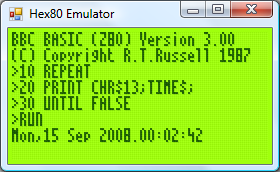
BBC BASIC can access the clock via the TIME$ pseudo-variable. This string variable returns the date and time in the format Sun,14 Sep 2008.15:20:00, and you can set the clock by assigning to the variable. When setting the clock you can specify either the date, the time, or both. Parsing the string has been an interesting exercise in Z80 programming, as it's not something I've ever attempted without regular expressions before!
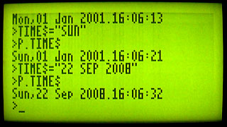
The only hardware modification since last time is a very poorly implemented software control of the backlight. The fifth bit of the control port specifies whether the backlight is on or off, and it can be toggled with the *BACKLIGHT command. I say "poorly implemented" as the transistor driver I'm using to interface the hardware port with the backlight LEDs results in a much dimmer backlight than when I had the LEDs hooked up directly to the power supply (on the positive side, at least the 5V regulator's heatsink is cool enough to touch - the backlight draws a lot of current).
Calling off-page functions
Now that I have access to all eight 16KB "pages" that make up the 128KB OS ROM, it may help to explain how one can use all of this memory. After all, if page 1 is swapped in and you wish to call a function on page 2, a regular Z80 call isn't going to work as you need to swap page 2 before calling the function then swap page 1 back in afterwards.
The trick is to exploit the way that the Z80 handles calling subroutines. There is a 16-bit register, PC, which stores the address of the next instruction to execute. When you call a subroutine, the Z80 pushes PC onto the stack then sets PC to the address of the subroutine. When you return from a subroutine (via the ret instruction) the Z80 simply pops the value it previously pushed onto the stack and copies this back to PC. Instead of calling the target subroutine directly, you call a special handler that is available on every page. Following your call is 16-bit identifier for the off-page function you wish to call. This handler then (prematurely) pops off the return address from the stack, reads the 16-bit value that follows it (which is the indentifier of the function you wish to call), looks up the page and address of the target function, swaps in the correct page and calls it as normal. When the function returns, the handler then swaps back the calling page and jumps back to the return address.
The Z80 has a series of rst instructions that call fixed addresses within the first 256 bytes of memory. These instructions are useful as they're small (one byte vs three bytes for a regular call) and fast, so I'm using rst $28 to call the off-page call handler (for no other reason than it's the same as the handler on the TI-83+).
As an example, let's say you had this function call at address $2B00:
$2B00:    rst $28
$2B01:    .dw $30F0
$2B03:    ; We'd return here.
When the Z80 executed that rst $28 it would push $2B01 (address of the next instruction) to the stack then jump to $28. The handler at $28 would do something like this:
    pop hl    ; hl is a 16-bit register and would now contain $2B01
    ld e,(hl) ; Read "e" from address pointed to by hl, now equals $F0
    inc hl    ; hl = $2B02
    ld d,(hl) ; Read "d" from address pointed to by hl, now equals $30
    inc hl    ; hl = $2B03 ("real" return address)
    push hl   ; push hl back on the stack so when we return from here we end up in the correct place.
Now, de is $30F0 - this is the identifier of the function we're calling. In my case, the identifier points to a function table on page 0. Each entry in the table is three bytes - one byte for the page index and two bytes for the address of the function on the that page. We'd need to do something like this:
    in a,(Page)  ; Read the current page into A.
    push af      ; Push A and F to the stack for later retrieval.
    and ~7       ; Mask out the lower three bits of the address.
    out (Page),a ; Sets current ROM page to 0.
    ex de,hl     ; Exchanges de and hl, so hl now points to the function identifier.
    or (hl)      ; ORs contents of memory at (hl) (ie, page number) with a, to set the target page.
    inc hl
    ld e,(hl)    ; e = LSB of target address
    inc hl
    ld d,(hl)    ; d = MSB of target address
    ex de,hl     ; hl = target address.
    out (Page),a ; Swaps in the correct page.
    ld de,ReturnFromHandler ; Address to return to.
    push de ; Store on stack.
    jp (hl) ; Set pc = hl.
ReturnFromHandler
    ; Swap back the original page which was pushed earlier...
    pop af
    out (Page),a
    ret ; ...and return to the calling page!
A further advantage of using rst $28 to replace call is that both are the same size, so the assembler can check if you're calling an address on the same page or a different one and insert the regular (and much faster) Z80 call in places where you don't need to swap the page.
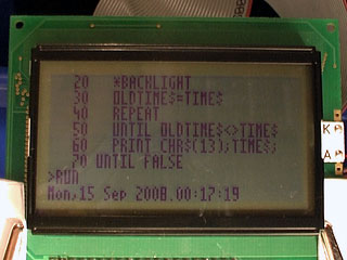
Finally, the obligatory video, this time showing a clock that toggles the backlight once a second.
Bank-Switching Memory and I2C
Thursday, 11th September 2008
Cheers for the comments. As EasilyConfused pointed out, I have done calculator programming in the past, which makes this much easier - learning Z80 assembly to program a calculator influenced the choice of CPU in this computer, and porting BBC BASIC to the calculator showed that with a minimal amount of code to sit between it and the hardware you'd have a decent operating system with very little work. And if a Terminator-related name is good enough for the UK military, it should be good enough for this project...
The I/O board from a few posts ago has undergone a few revisions:
Both PS/2 ports are now fully wired up, though only the lower one is currently used by the OS for keyboard input. I will need to adjust the AT protocol routines (the AT protocol is used to control both keyboard and mouse) to support multiple physical ports, as it was adapted from code I wrote for the TI-83+ calculator and as such only supports one device at a time. The mouse position will be polled by calling ADVAL(axis%), which on the BBC Micro would return the joystick position (axis% specifies the type of information to retrieve from the mouse - a value of 0 returns the buttons as a bitfield, 1 returns the movement in the X axis, 2 the movement in the Y axis and 3 the amount the scrollwheel has been scrolled).
At the very bottom of the circuit board is another 8-bit latch. This is for the (currently) write-only control port. The three least significant bits specify the current ROM page (one of eight 16KB ROM pages can be swapped in for a total of 128KB) and the next bit specifies one of two 16KB RAM pages accessible in the $4000..$7FFF address range. One of the other bits will be used to switch the LCD backlight on and off in software, one more may be connected to a buzzer, and I'm sure I can find some use for the last two. As it's write-only, its current state needs to be stored in RAM so that you can change bits of it (eg when changing the ROM page you wouldn't want to change the backlight status at the same time; you'd need to retrieve the current state and mask in the bits you wish to preserve). This is obviously an ugly hack, and I'm hoping I'll be able to use some of the space to the right of the latch IC on the circuit board to add the other latch to allow the port to be read as well (an I/O port needs two latches - an output latch that takes data from the data bus and outputs it to external hardware, and an input latch that takes data from external hardware and puts it back on the data bus).
The first test of the new ROM paging hardware was to display a simple animation. Assuming 1KB on each ROM page was taken up by the animation playback program, that leaves 15KB per ROM page. A frame (128×64 pixels) is 1KB, so that's 15 frames per page, or 120 frames total. I converted a clip from Pink Floyd's Arnold Layne music video to a suitable format and wrote a playback routine that could run from RAM. When the computer booted it would copy the player to RAM and run it from there as it could then run uninterrupted when different ROM pages were swapped in to read the frame data.
An animation like this is a useful test, as if the ROM paging didn't work properly (simulated by holding the three ROM page selection lines low) the software would still run, but would just loop the first 15 frames (or play chunks of 15 frames out of sequence) instead of crashing.
Another addition to the circuit above is the cluster of discrete transistors and resistors under the lowest PS/2 port. This is the same sort of pair of open-collector I/O data lines that drive each PS/2 port, except that the two data lines are fed out of the I/O board and back to the breadboard that's currently sitting between the memory board and the I/O board to these two simple 8-pin chips:
This is the I2C bus, a simple, low-speed, two-wire bus that will allow other components be easily connected to the computer. The I2C protocol is implemented in software. The two chips in the above image are a DS1307 real-time clock (foreground, with quartz crystal) which I hope to use for timing purposes and a 24LC256 32K×8 EEPROM which I hope to use for file storage. I would need to have some way of accessing the I2C bus externally (to plug in EEPROMs as removable storage) as well as supporting the internal devices.
I haven't yet done any work on supporting I2C devices properly, but I have added I2C bus emulation to the emulator I'm using to develop the OS. BBC BASIC will pass commands prefixed with a *STAR to the operating system, so I've added a *I2CPROBE command that will hammer through all available addresses and list any devices that acknowledge a write request.
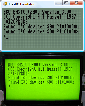
$A0 is the EEPROM and $D0 is the clock.
I think I may have dug myself into a hole for CPU timing. I mentioned that I will need to drop the CPU clock to 2MHz when accessing the LCD; unfortunately, switching between 2MHz and 10MHz doesn't seem to work very well. I can run the system relatively stably at either speed (though at 10MHz data sent to the LCD is occasionally corrupted) but if I try and switch dynamically (eg switching from the 10MHz to the 2MHz clock when /IORQ goes low to indicate an I/O request) the system locks up. My assumption is that during time it takes the logic gates that perform the 10MHz/2MHz switch to properly settle into their new state (which is in the tens of nanoseconds) the clock signal stutters a little, effectively producing a clock signal (albeit a brief one) well over 10MHz. I don't have an oscilloscope to verify this, however. 
Running BBC BASIC on a home-built computer
Sunday, 7th September 2008
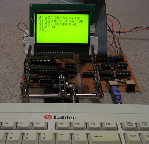
This computer needs a name - I'd welcome any suggestions!
I have built a circuit on another piece of stripboard that will handle memory, clock signal generation and the Z80 itself.
A few posts ago I was wondering about how I'd partition memory. To date I've been using a very simple circuit where the lower 32KB of addressable memory is mapped to ROM and the upper 32KB is mapped to RAM. As my ROM chip is 128KB and I have two 32KB RAM chips, this seems a bit wasteful.
The memory layout I'm now using is quite simple: the upper 32KB is still mapped to RAM. However, only the first 16KB is mapped to ROM, and the three most significant bits of the ROM chip's address lines are connected to a device on the I/O board so that one of its eight 16KB "pages" can be swapped in. The next 16KB will be mapped to RAM, and the most significant bit of the RAM chip's address is connected to the same device on the I/O board so one of its two 16KB "pages" can be swapped in.
For more information, see the Wikipedia article on bank switching. There is a potential problem here; the Z80 uses particular fixed addresses for certain operations. The three most obvious ones are $0000 (jumped to on reset), $0038 (address of maskable interrupt handler) and $0066 (address of non-maskable interrupt handler). As which 16KB bank switched in at power-on is effectively random, the easy way around this problem is to ensure that the first 256 bytes or so of every ROM page has the same code assembled on it. This means that whichever page is swapped in on boot doesn't matter, as the same common boot code is available on each page.
The assembled memory board looks like this:
;if(img.style.backgroundImage){img.style.backgroundImage='url('+img.src+')';img.src=imgs[img.src.indexOf(imgs[1])<0?1:2]}else{img.style.backgroundImage='url('+img.src+')';img.src=imgs[2];};void(0);)
I have only attached one of the 32KB RAM chips. The wiring was becoming a bit of a nightmare (I think I'll need to solder to the track side of the stripboard to fit in that other RAM chip) so for the moment the system can only access the fixed 32KB RAM. I haven't yet added the device on the I/O board to handle bank switching, so for the moment the ROM is permanently configured to access the first 16KB page by pulling the its three externally controllable address lines low.
That said, this machine does genuinely run BBC BASIC (the last system only ran a mockup with a dummy header at the top of the screen). I've done quite a bit of work on the OS in the emulator and it works pretty well there, and with a minor adjustment to cram it onto a single 16KB page it works well on hardware too.
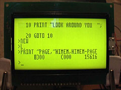
The row of chips along the bottom of the memory board are responsible for generating the clock signals that drive the computer. If this looks needlessly complex, that's because it can run at either 10MHz or 2MHz and generates the E signal for LCD access. The CPU needs to drop to 2MHz when accessing the LCD (the LCD driver can't keep up, otherwise) so I'll probably end up connecting the input for this 2MHz/10MHz switch to the LCD chip enable pins so that normally the system runs at 10MHz but drops to 2MHz when accessing the LCD. Allowing the user to drop to 2MHz to save power is an appealing idea, however...
2MHz should be enough for anyone
Wednesday, 27th August 2008
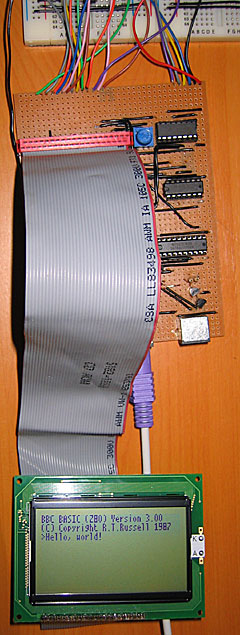 LCD Timing
Last time I discussed the hardware I mentioned I had LCD timing issues. I have finally resolved them, but this has been the most time consuming part of the project so far.
The first thing to sort out was the LCD's E pin. Once you have set up the LCD's input pins to a state where they're ready to read or write data, you need to drive this pin high. I had had some success by holding it high permanently and relying on the Z80 to set all the other to the right state at roughly the same moment, but this was inaccurate and resulted in occasional display glitching.
Consulting the datasheet, it appears that once the input pins are ready E needs to be held low for at least 450nS and then needs to be driven high for at least 450nS. Hmm. During an I/O request (and once the Z80 has prepared the address and data bus) there's a delay of 1 clock cycle, then /IORQ is held low for about 2.5 CPU cycles. That is the window of opportunity. I have connected a binary counter to the Z80's clock signal and take the least significant bit of the output - every clock cycle this output toggles between a low and a low, effectively halving the CPU clock rate. I then connect the counter's reset pin (which overrides the clock input and forces it to output zero) to /IORQ. The result is that when the Z80 is not accessing hardware the counter is held in its reset state, and E is held low. When the Z80 holds /IORQ low, the counter starts up and outputs a zero for one CPU cycle, outputs a one for the next CPU cycle, then outputs a zero for the next half clock cycle at which point /IORQ goes high again and it is back to zero anyway. This is exactly what's needed!
This also allows us to calculate the maximum CPU clock rate. If we are generous and allow E to be low for 500nS then high for 500nS, that gives us a CPU clock rate of 1/500nS=2MHz.
Anyhow, that's one problem resolved, but there was still one nasty bug. When reading from the LCD it would occasionally end up writing to the area that was being read or, in worse cases, the Z80 would "crash". The LCD has a R/#W pin that is held high when reading and held low when writing. I had connected it directly to the Z80's /WR pin, which is high normally and low when writing. The problem here is "normally" as the LCD was expecting to be read even when the Z80 wasn't requesting a /RD. When being read, the LCD expects to put something onto the data bus, and it appeared that it kept thinking that it needed to put something on the bus when it wasn't needed. This caused fighting with the other chips that were trying to put their own values on the data bus, hence the crashes as the Z80 received invalid data.
The answer was very easy; simply connect the Z80's /RD pin to the LCD's R/#W pin via a NOT gate. In the default state the pin is held low (LCD expects a write and leaves the data bus alone), and only goes high during a /RD. The LCD interface is now very robust.
CPU Clock
Above I mention the calculation for the maximum clock rate. Rather than use the 555 for timing, I switched to using a 10MHz crystal resonator oscillator. I'm using the serial resonant circuit from z80.info with a 74F04 hex inverter (second circuit down). Fortunately the counter chips I have are decade counters (ie, designed to count from 0 to 9) made up of a ÷2 and a ÷5 section. I can connect a 10MHz oscillator to the ÷5 section and use the output of that to drive the CPU. In the final design I'd like to add a "hardware control port" with a bit that would let the programmer choose 2MHz or 10MHz mode by setting or resetting a particular output bit (other control bits would include switching the LCD backlight on or off and a buzzer for beeping sound output).
PS/2 Ports
As a friend pointed out, the 8-bit open-collector I/O port (which will drive two PS/2 ports, the I2C bus and TI calculator link port) had a flaw - there was no resistor on the base of the output transistors. The result is that if the output latch tries to drive the transistor base high, the transistor switches on and shorts the output of the latch to ground. This was clearly a problem in the design as the LCD backlight dimmed when trying to output to these ports as they drew a excessive amount of current when effectively short-circuited. A 22K resistor between the output latch and base of the transistor fixed the problem.
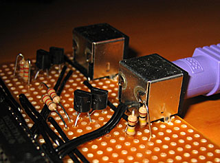
In the above photo, I've also added two 100K resistors to hold the output high when floating, but only to the foreground PS/2 port for the time being. I don't think I'll be controlling a mouse yet!
Revised OS
With a little modification of the Emerson PS/2 library I've got a basic keyboard driver up and running on the hardware. All the OS does for the moment is check for keys and display them on the screen. It's currently hard-coded to the UK layout, as I haven't yet decided how I'm going to handle storage and by keeping the layout in ROM it at least frees up a few hundred bytes of RAM that would otherwise need to be there for the scancode translation tables.
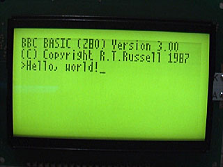
Remapped IO.DLL
Sunday, 24th August 2008
A common problem with software that uses the parallel port is that is hard-coded to use particular port addresses, such as 0x378 for LPT1. This is all well and good on older machines that have integrated or ISA ports that can be assigned this base address, but newer machines with PCI cards don't get any choice over which port address range is assigned to the parallel port.

The supporting software for the Willem programmer has this problem, and so far I've been using an old XP laptop with a flaky WiFi adapter to program chips. This has been rather painful, understandably!
Fortunately, in Windows NT Microsoft forbade us from accessing hardware ports directly when in user-mode. This probably doesn't sound very fortunate, but the result is that various libraries for accessing the I/O ports using an embedded kernel-mode driver sprang up. Whilst this still isn't perfect (you need to run the calling app with Administrator privileges) it does mean that apps that access the parallel port will have one of these libraries kicking around as a DLL in their installation directory. The Willem programmer software is no exception; it uses IO.DLL.
The trick, then, is to simply replace the IO.DLL bundled with the app with a custom one that performs the same task, but redirects port writes in the LPT1 range (0x378~0x37F) to a user-specified base address (in my case, 0xCCD8). I couldn't get IO.DLL itself to work from within a DLL, and using it meant that you'd have to also rename the existing IO.DLL to something else, so I used Inpout32.dll instead to access the ports from the new DLL.
IO.DLL provides many helper functions, Inpout32.dll only offers two - Inp32() and Out32(). Fortunately, the Willem software doesn't seem to use any of the helper functions, and only uses PortIn() and PortOut(). (It does also use IsDriverInstalled(), but I've hard coded that to always return -1). The sample C++ interface code doesn't check the return value of GetProcAddress(), so the software still initialises, but will crash with an access violation if it tries to use any of the unsupported functions.
With some help from ibutsu to get around the C function name mangling problem (resolved by adding a simple .def file), you can simply extract three files into the Willem software directory (new io.dll, inpout32.dll for port access and io.ini for the user-specified port address) and the software appears to work fine! (I haven't tested all chip modes, as I only have one type of flash memory chip and an I2C serial EEPROM, but they work).
Download DLLs and source or documentation.
Z80 computer with a primitive I/O board
Wednesday, 20th August 2008
A computer needs some way of interacting with the outside world via input and output devices. It's about time, then, that the Z80 computer project acquires a section dedicated to I/O.
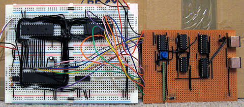
The Z80 differentiates between memory and I/O devices, though both share the data bus and the address bus. You can control I/O devices using the in (input) and out (output) instructions. When you input or output you must specify a device address and a value or target register. For example,
    in a,($20) ; Read a value from device $20 and store it in A.
    ld a,123
    out ($40),a ; Output 123 to device $40.
When you write to a device, the following happens:
- The address bus is set to the address of the device to output to.
- The data bus is set to the value to be written to the device.
- The /IORQ and /WR pins on the Z80 go low.
- The device processes the written data.
- The /IORQ and /WR pins on the Z80 go high.
Reading from the device is very similar:
- The address bus is set to the address of the device to read from.
- The /IORQ and /RD pins on the Z80 go low.
- The device puts the value to read onto the data bus.
- The Z80 reads the value on the data bus.
- The /IORQ and /RD pins on the Z80 go high.
(Accessing memory is a similar procedure, except with the /IORQ pin replaced by the /MREQ pin).
Interfacing I/O devices to a Z80 CPU should be rather straightforwards, then. I am using a 74HCT138N 3-to-8 line inverting decoder to handle the address bus input and /IORQ signal. This IC has three address inputs and 8 outputs. If the address input is %000, output 0 is low and all the other pins are high; if the address input is %001 output 1 is low and all the others are high; if the input is %010 output 2 is low and all the others are high (and so on and so forth). /IORQ is connected to another input on the chip, /E1, which causes all of the pins to go high when it is high regardless of the address input.
What does this mean in practice? Well, most devices have a "chip enable" or "chip select" input pin. When this input is active the device performs its function, but when the input is not active the device is deactivated and doesn't respond to any other inputs or output anything. By connecting each output of the 3-to-8 decoder to a particular device's chip enable pin I can ensure that each device is only activated when its address is specified on the address bus and the /IORQ pin on the Z80 is low.
I have connected the Z80's A5-A7 to A0-A2 on the 3-to-8 decoder. This means that the first device has a base address of $00, the second $20, the third $40 and so on at increments of $20. This might sound a little odd, but has a reason. Some devices, such as the LCD, have sub-addresses of their own. In the case of the LCD, it has a pin that specifies whether you're dealing with an instruction (such as a command to switch the display on or off or read the LCD status) or some data (which forms part of the picture on the LCD). By attaching this pin directly to the Z80's A0 and the LCD's chip select pin to output 1 from 3-to-8 decoder you end up with an LCD instruction port at $20 and an LCD data port at $21.
An LCD is all well and good, but we'll need to take input from the user. To accomplish this, I'm going to supply two PS/2 ports and implement the AT protocol (as used by PS/2 keyboards and pointing devices) in software. Each device only requires two open-collector data lines (data and clock), so a single I/O device that provides eight I/O lines would be useful.
The design I'm going for uses two 74AC373 octal transparent latches. When the latch enable input pin is held high whatever value is on the input passes through to the corresponding output. When the latch enable pin goes low, the last value that was latched at the input is still output. These particular latches also have an output enable pin that can be used to disable the outputs and let them "float" (ie, other devices can then drive that particular connection high or low as required). In this instance, one latch has its output enable pin activated so that it always outputs the last value written to it and has its latch enable pin connected to the Z80's /WR pin. The other latch has its latch enable pin activated so that it always outputs the values at its input and has its output enable pin connected to the Z80's /RD pin.
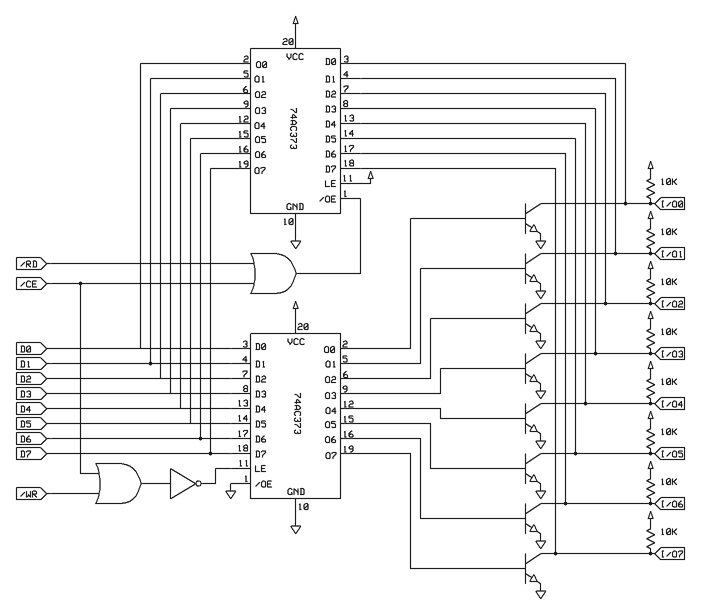
The transistors on each output are used to provide open-collector outputs. When the base of the transistor is held low, the transistor is "switched off" and its output floats, and so can be driven by external circuitry. When the base of the transistor is held high, it switches on and effectively connects the output to ground. A pull-up resistor ensures that the pin has a high signal when not connected to anything. This arrangement is useful as each pin can be driven low by either device and so works as an input or an output (for a real-world example, an AT keyboard usually outputs a clock signal on one line to the host when sending data, but if the host pulls the clock line low it can inhibit communication and the keyboard buffers the data to send instead).
;if(img.style.backgroundImage){img.style.backgroundImage='url('+img.src+')';img.src=imgs[img.src.indexOf(imgs[1])<0?1:2]}else{img.style.backgroundImage='url('+img.src+')';img.src=imgs[2];};void(0);)
Rather than build the circuit on breadboard, I went straight to stripboard. The above photo shows an incomplete version of the output board. Only one PS/2 port is wired up at all! The pin header to the left is to connect the LCD to. The coloured wires at the extreme left connect this I/O board to the rest of the computer.
;if(img.style.backgroundImage){img.style.backgroundImage='url('+img.src+')';img.src=imgs[img.src.indexOf(imgs[1])<0?1:2]}else{img.style.backgroundImage='url('+img.src+')';img.src=imgs[2];};void(0);)
I have modified the Z80 board I was using last time to add support for RAM. The 3-to-8 decoder in the bottom right is used to partition the address space into two 32KB regions. The lower 32KB is mapped to ROM, and the upper 32KB is mapped to RAM. This wastes 75% of the ROM chip (it's a 128KB chip) but without a more complex memory management unit this will have to do for the moment. The most significant bit of the address bus, A15, is fed into the 3-to-8 decoder along with the /MREQ pin.
The test software is a Z80 program that displays an animation on the LCD using 20 frames (1KB per frame) stored in ROM.
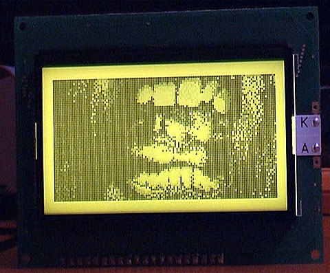
The Z80 is still not breaking MHz speeds, but there are problems here. I have not interfaced the LCD correctly, as its timing patterns for reading and writing data are quite different to those used by the Z80. Bizarrely, holding the E pin on the LCD permanently high appears to work 99% of the time, even though the datasheet indicates that it should be used to clock data in or out. The result is glitches in the data sent to the LCD, usually on the left hand side (the left hand side of the display has a propensity to believe it's been sent the "switch off" command). I'm not sure I'll be able to remedy this situation. Judging by the datasheet it looks like the LCD does its stuff when the E pin goes from a low to high state (the Z80 does everything when /IORQ goes low), so maybe simply inverting /IORQ and pumping it into E will do the trick.
Z80 Light-flasher
Wednesday, 13th August 2008
Now armed with a flash programmer, I thought it about time to try and build a Z80-based system.
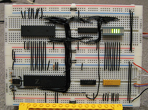
Not much to look at, and it doesn't do much either. The large IC in the bottom-left, prominently marked Z, is the Z80 itself. To its left is a 555, generating a ~220Hz clock signal (yes, Hz, not MHz or even kHz). Above the Z80 is another large chip - this is the 128KB flash ROM. The eight parallel wires between them are the address bus - only A0 to A7 are connected. This only lets the Z80 address 256 bytes, but that should be enough for testing.
To the right of the flash ROM is an octal latch. This is used to provide an 8-bit output port for the system, which is connected to the LEDs to its right. As the latch's latch enable pin is active high, unlike everything else in the system (which is active low - ie, it does something when you drive it low) I have to put a NOT gate - the final black IC to the right of the Z80 - between it and the Z80's /WR (write) pin. I do not do any address decoding or even check the /IORQ pin, so any value written to to any hardware device or memory address will end up on the LED display. Not that that really matters, as there is a conspicuous lack of RAM in the system!
The large physical size and tedium of wiring even such a primitive system as this makes me wonder whether it's worth jumping straight to stripboard for subsequent hardware revisions...
For the curious, the program running on the Z80 is as follows.
.for p = 0 to 7
.defpage p, kb(16), $0000
.loop
.emptyfill $FF

.page 0

	im 1
	di

--	ld hl,LightSequence
	ld b,LightSequenceEnd-LightSequence
-	ld a,(hl)
	out (0),a
	inc hl
	djnz -
	jr --

LightSequence
	.db %00000001
	.db %00000010
	.db %00000100
	.db %00001000
	.db %00010000
	.db %00100000
	.db %01000000
	.db %10000000
	.db %01000000
	.db %00100000
	.db %00010000
	.db %00001000
	.db %00000100
	.db %00000010
	.db %00000001
	.db %00000010
	.db %00000100
	.db %00001000
	.db %00010000
	.db %00100000
	.db %01000000
	.db %10000000
	.db %01000000
	.db %00100000
	.db %00010000
	.db %00001000
	.db %00000100
	.db %00000010
	.db %00000001
	.db %00000011
	.db %00000111
	.db %00001111
	.db %00011111
	.db %00111111
	.db %01111111
	.db %11111111
	.db %11111111
	.db %00000000
	.db %11111111
	.db %00000000
	.db %11111111
	.db %00000000
	.db %11111111
	.db %00000000
	.db %11111111
	.db %00000000
	.db %11111111
	.db %00000000
	.db %11111111
	.db %11111110
	.db %11111100
	.db %11111000
	.db %11110000
	.db %11100000
	.db %11000000
	.db %10000000
	.db %00000000
	.db %10000000
	.db %11000000
	.db %11100000
	.db %11110000
	.db %01111000
	.db %00111100
	.db %00011110
	.db %00001111
	.db %10000111
	.db %11000011
	.db %11100001
	.db %11110000
	.db %01111000
	.db %00111100
	.db %00011110
	.db %00001111
	.db %10000111
	.db %11000011
	.db %11100001
	.db %11110000
	.db %01111000
	.db %00111100
	.db %00011110
	.db %00001111
	.db %00000111
	.db %00000011
	.db %00000001
	.db %00000000
LightSequenceEnd

.echoln strformat("Size: {0} bytes", $)
Emulators and neatened wiring
Tuesday, 12th August 2008
I've decided to switch to a regular 10MHz Z80 rather than a Z180, given the difficulty of using an SDIP 64. I now have a DIP 40 Z80 ready for use, but as I don't have the programmer for the Flash chip (which will hold the OS) there's not much I can do with it physically. I have therefore cobbled together a basic emulator to help develop some of the software beforehand.
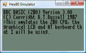
To cut hardware costs I'm going to try and handle input in software. One bit of hardware I'm planning on having is an eight-bit open collector I/O port. Open collector pins float high in their reset state, and any device connected to the pin can drive it low. AT devices (keyboard and mouse) use this type of electrical connection, as does the I2C bus and the TI calculator link port. I can use up the eight pins easily - two pins per AT device (keyboard and mouse) makes four, two pins for the I2C bus and two pins for a TI calculator link port.
The I2C bus I mentioned above is a simple way to enhance the computer once built. There will be one device permanently attached to the bus, a DS1307 real-time clock, which will be used to provide time-keeping functions for the OS as well as generating periodic interrupts (the chip could be configured to trigger an interrupt 100 times a second, useful for timing game logic). I could then leave empty space on the circuit board to add other I2C devices over time, or have a socket on the case that could be used to plug in additional I2C modules.
Now that I have some more tools, namely a desoldering pump, I tidied up the horrible hack job I'd done on the graphical LCD (replacing the multiple wires with a single pin header).
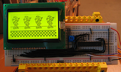
Yes, still the PICAXE here, but I'm using its 256 byte EEPROM to store a 32×64 pixel image of Sonic that is repeated four times horizontally.
I'm still not sure what I'm doing with regards to memory or storage. I'm still working on the simple assumption that ROM is 32KB ($0000..$7FFF) and RAM is 32KB ($8000..$FFFF) but this wastes a lot of memory and isn't very flexible at all. I've planned a bank-switching MMU, but as this will require at least four registers to store what appears in each of the four 16KB windows it will end up being physically very large and painful to wire.
As for storage, I have no idea. I have some 32KB I2C EEPROMs, but 32KB isn't exactly very large. Alternatively, I have an old 512MB SD card, and could try talking to it over bit-banged SPI. (SD cards use 3.3V, though, which complicates matters - not to mention that bit-banged SPI is going to be a little sluggish). I also have a USB module which can talk to USB mass storage devices over a serial connection, so maybe I should add a UART to the project. Adding a fully-blown USB module (which also plays WMA, MP3 and MIDI files) to such an otherwise low-tech computer feels like heresy, though.
Experimenting with a 32KB RAM
Monday, 4th August 2008
The next component I thought I'd experiment with is the RAM. The project is an analogue recorder - a circuit that samples an analogue input periodically and saves it in RAM, and can be configured to play the recorded signal back afterwards.
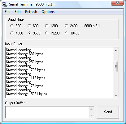
Yes, it says plating.
A single RAM chip offers 32K with an eight-bit word size. This requires fifteen lines to address it, A0..A14. The PICAXE-28X1 that is to control the circuit does not have enough output pins to be able drive this address bus and a data bus (to transfer values to and from RAM) and a still have enough pins left over to control the various components. To get around this, two octal (eight-bit) latches are used to drive the address lines, A0..A7 from one chip and A8..A14 from another. The inputs to these latches are connected to the data bus (PortC on the PICAXE), and two pins on the PICAXE are set aside to trigger the latch enable pins on either latch.
What this means in practice is that if you wished to change the current address to $1234 you would put $34 on the data bus and trigger the latch that corresponds to the least significant byte of the address, then put $12 on the data bus and trigger the latch that corresponds to the most significant byte of the address.
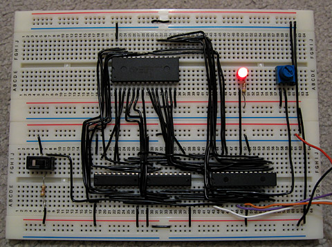
Any hobbyist can have wire insulation in any color that he wants so long as it is black.
A 10K potentiometer provides the required analogue input and an LED provides the output. The switch on the left is used to change between recording and playback modes. The large chip at the top is the RAM, the two small ones in the middle are the octal latches and the medium one on the right is the PICAXE-28X1.
As only 15 lines are needed to address 32KB, the most significant bit of the address bus is wired to the /WE pin of the RAM chip. This pin determines whether we're writing to (low) or reading from (high) the chip. This effectively means that addresses $0000..$7FFF are used when writing and addresses $8000..$FFFF are used when reading.
The only remaining connections to the RAM chip required are chip enable (/CE) and output enable (/OE). When chip enable is low, the RAM chip can be accessed; when high, it ignores all input. When not in use we therefore make sure that chip enable is high. When output enable is low, the RAM chip puts the value at the current address onto the data bus, so we need to pull this low when reading but make sure it's left high most of the time so that the RAM chip doesn't interfere with other devices trying to put a value on the data bus.
The code for the test program is as follows:
; Pins:
Symbol RamChipDisable   = 4
Symbol RamOutputDisable = 5
Symbol AddressLatch0    = 6
Symbol AddressLatch1    = 7

; Registers:
Symbol RamValue         = B0
Symbol RamAddress       = W1 ; B3:B2
Symbol RamAddressLow    = B2
Symbol RamAddressHigh   = B3
Symbol RamPointer       = W2 ; B5:B4

Symbol RecordingLength  = W3 ; B7:B6

Boot:
	Let DirsC = $00
	High RamChipDisable
	High RamOutputDisable
	Low AddressLatch0
	Low AddressLatch1
	Let RamPointer = 0
	SetFreq M8

Main:

StartPlaying:
	SerTxd ("Started playing: ", #RecordingLength, " bytes", CR, LF)
	Let RamPointer = 0
	Pause 100
PlayingLoop:
	If PortA Pin1 = 1 Then StartRecording

	; Read stored value from RAM.
	Let RamAddress = RamPointer
	GoSub ReadRam

	; Set LED brightness to stored value.
	Let W4 = RamValue * 4
	HPwm PwmSingle, PwmHHHH, %0100, 255, W4

	; Increment playback pointer and loop if hit end.
	Let RamPointer = RamPointer + 1
	If RamPointer = RecordingLength Then
		RamPointer = 0
	EndIf

	; Loop back.
	GoTo 	PlayingLoop


StartRecording:
	SerTxd ("Started recording...", CR, LF)
	Let RecordingLength = 0
	Pause 100
RecordingLoop:
	If PortA Pin1 = 0 Then StartPlaying

	; Read value from ADC.
	ReadAdc 0, RamValue

	; Set LED brightness to read value.
	Let W4 = RamValue * 4
	HPwm PwmSingle, PwmHHHH, %0100, 255, W4

	; Store value read from ADC into RAM.
	Let RamAddress = RecordingLength
	GoSub WriteRam

	; Increment record pointer.
	Let RecordingLength = RecordingLength + 1

	GoTo RecordingLoop

WriteRam:
	; Set up address bus:
	Let DirsC = $FF
	Let RamAddressHigh = RamAddressHigh & %01111111
	Let PinsC = RamAddressHigh
	High AddressLatch1 : Low  AddressLatch1
	Let PinsC = RamAddressLow
	High AddressLatch0 : Low  AddressLatch0
	; Set up data bus and write:
	Let PinsC = RamValue
	Low RamChipDisable
	High RamChipDisable
	Let DirsC = $00
	Return

ReadRam:
	; Set up address bus:
	Let DirsC = $FF
	Let RamAddressHigh = RamAddressHigh | %10000000
	Let PinsC = RamAddressHigh
	High AddressLatch1 : Low  AddressLatch1
	Let PinsC = RamAddressLow
	High AddressLatch0 : Low  AddressLatch0
	; Set up data bus and read:
	Let DirsC = $00
	Low RamOutputDisable
	Low RamChipDisable
	Let RamValue = Pins
	High RamChipDisable
	High RamOutputDisable
	Return
As before, there's a simple video of the circuit in action.
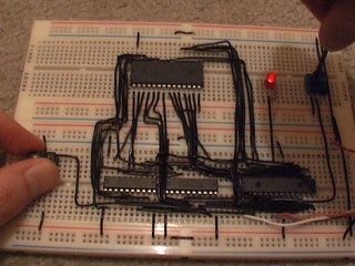
Back to Hardware
Friday, 1st August 2008
I enjoy dabbling with low-level programming, but have never actually built a computer to run these programs. I think it's time to correct that, and as the BBC BASIC project has required me to develop an almost complete Z80 OS (the only thing that's left for the TI-OS to do is manage files) I thought a Z80 computer would be a good start.
The planned specs are (as a starting point):
- 10 MHz Z80180 CPU;
- 64KB RAM (2 32K×8 SRAM chips);
- 128KB Flash ROM;
- Graphical LCD;
- Simple joypad input;
- Keyboard input (AT using either software AT routines or dedicated microcontroller).
The first spanner in the works is the Z80180, as I didn't read the datasheet closely enough and it's in a DIP 64 package with 0.07" pin spacing instead of the standard 0.1" pin spacing. I'll need to find some way of constructing an adapter so I can use it with my breadboards and stripboard.
In the meantime, I've concentrated on the graphical LCD. I picked a 128×64 backlit graphical LCD for the princely sum of £16. It's very easy to control - you hook up it up to a 8-bit data bus to transfer image data and instructions and a handful of control pins to indicate what you're doing on that bus (reading or writing, whether you're sending an instruction or some image data, that sort of thing) and that's it - the only supporting circuitry it requires is a 10K potentiometer to act as a contrast control and power for the display and backlight.
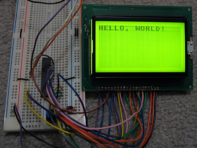
To experiment with the LCD, I'm using a PICAXE-28X1 microcontroller, programmed in BASIC. There isn't much space to store graphics, so I'm using a 32 character font (at eight bytes per character, that takes up all 256 bytes of free EEPROM space!)
; LCD data bus should be connected to port C.

Symbol LcdRegisterSelection = 0 ; D/I  :  4
Symbol LcdReadWrite         = 1 ; R/W  :  5
Symbol LcdStartEnable       = 2 ; E    :  6
Symbol LcdChipSelect1       = 3 ; CS1  : 15
Symbol LcdChipSelect2       = 4 ; CS2  : 16
Symbol LcdReset             = 5 ; /RST : 17

; Storage for console state variables.

Symbol ConsoleX             = B10
Symbol ConsoleY             = B11
Symbol ConsoleChar          = B12


	GoSub LcdInit                              ; Initialise LCD.
	B0 = %00111111 : GoSub LcdWriteInstruction ; Switch LCD on.

	GoSub LcdClear ; Clear LCD

	; Write the obligatory message to the LCD.

	ConsoleX = 0 : ConsoleY = 0

	ConsoleChar = $08 : GoSub LcdPutChar ; H
	ConsoleChar = $05 : GoSub LcdPutChar ; E
	ConsoleChar = $0C : GoSub LcdPutChar ; L
	ConsoleChar = $0C : GoSub LcdPutChar ; L
	ConsoleChar = $0F : GoSub LcdPutChar ; O
	ConsoleChar = $1D : GoSub LcdPutChar ; ,
	ConsoleChar = $00 : GoSub LcdPutChar ;
	ConsoleChar = $17 : GoSub LcdPutChar ; W
	ConsoleChar = $0F : GoSub LcdPutChar ; O
	ConsoleChar = $12 : GoSub LcdPutChar ; R
	ConsoleChar = $0C : GoSub LcdPutChar ; L
	ConsoleChar = $04 : GoSub LcdPutChar ; D
	ConsoleChar = $1B : GoSub LcdPutChar ; !

	Pause 2000

	B2 = 0
MainLoop:
	B2 = B2 - 1
	B0 = B2
	GoSub LcdGotoZ
	Pause 30
	GoTo MainLoop

LcdInit:
	DirsC = $00               ; Set data bus to input.
	High LcdStartEnable       ; We're not writing anything.
	High LcdChipSelect1
	High LcdChipSelect2
	Low LcdReset
	Pause 500
	High LcdReset
	Pause 500
	Return

LcdWriteInstruction:
	Low LcdReadWrite
	DirsC = $FF               ; Data bus = output.
	PinsC = B0                ; Set data bus state.
	Low LcdRegisterSelection  ; Instruction, not data.
	Low LcdStartEnable
	High LcdStartEnable
	DirsC = $00               ; Leave data bus floating.
	Return

LcdWriteData:
	Low LcdReadWrite
	DirsC = $FF               ; Data bus = output.
	PinsC = B0                ; Set data bus state.
	High LcdRegisterSelection ; Data, not instruction.
	Low LcdStartEnable
	High LcdStartEnable
	DirsC = $00               ; Leave data bus floating.
	Return

LcdGotoX:
	B0 = B0 And 7
	B0 = B0 + %10111000
	GoTo LcdWriteInstruction

LcdGotoY:
	B0 = B0 And 63
	B0 = B0 + %01000000
	GoTo LcdWriteInstruction

LcdGotoZ:
	B0 = B0 And 63
	B0 = B0 + %11000000
	GoTo LcdWriteInstruction

LcdClear:
	For B2 = 0 To 7
		B0 = B2
		GoSub LcdGotoX
		B0 = 0
		GoSub LcdGotoY
		B0 = 0
		For B3 = 0 To 63
			GoSub LcdWriteData
		Next
	Next B2
	Return

LcdPutMap:
	B1 = B0 * 8
	For B2 = 0 To 7
		Read B1, B0
		GoSub LcdWriteData
		B1 = B1 + 1
	Next B2
	Return

LcdPutChar:
	B0 = ConsoleY
	GoSub LcdGotoX
	B0 = ConsoleX * 8
	If B0 < 64 Then
		Low LcdChipSelect2
	Else
		Low LcdChipSelect1
		B0 = B0 - 64
	EndIf
	GoSub LcdGotoY
	B0 = ConsoleChar
	GoSub LcdPutMap
	High LcdChipSelect1
	High LcdChipSelect2
	ConsoleX = ConsoleX + 1
	If ConsoleX = 16 Then
		ConsoleX = 0
		ConsoleY = ConsoleY + 1
		If ConsoleY = 8 Then
			ConsoleY = 0
		EndIf
	EndIf
	Return

; Font
EEPROM $00,($00,$00,$00,$00,$00,$00,$00,$00,$7E,$7F,$09,$09,$7F,$7E,$00,$00)
EEPROM $10,($7F,$7F,$49,$49,$7F,$36,$00,$00,$3E,$7F,$41,$41,$63,$22,$00,$00)
EEPROM $20,($7F,$7F,$41,$63,$3E,$1C,$00,$00,$7F,$7F,$49,$49,$49,$41,$00,$00)
EEPROM $30,($7F,$7F,$09,$09,$09,$01,$00,$00,$3E,$7F,$41,$49,$7B,$3A,$00,$00)
EEPROM $40,($7F,$7F,$08,$08,$7F,$7F,$00,$00,$41,$41,$7F,$7F,$41,$41,$00,$00)
EEPROM $50,($20,$61,$41,$7F,$3F,$01,$00,$00,$7F,$7F,$1C,$36,$63,$41,$00,$00)
EEPROM $60,($7F,$7F,$40,$40,$40,$40,$00,$00,$7F,$7F,$06,$1C,$06,$7F,$7F,$00)
EEPROM $70,($7F,$7F,$0C,$18,$7F,$7F,$00,$00,$3E,$7F,$41,$41,$7F,$3E,$00,$00)
EEPROM $80,($7F,$7F,$09,$09,$0F,$06,$00,$00,$3E,$7F,$41,$31,$6F,$5E,$00,$00)
EEPROM $90,($7F,$7F,$09,$19,$7F,$66,$00,$00,$26,$6F,$49,$49,$7B,$32,$00,$00)
EEPROM $A0,($01,$01,$7F,$7F,$01,$01,$00,$00,$3F,$7F,$40,$40,$7F,$3F,$00,$00)
EEPROM $B0,($1F,$3F,$60,$60,$3F,$1F,$00,$00,$7F,$7F,$30,$1C,$30,$7F,$7F,$00)
EEPROM $C0,($63,$77,$1C,$1C,$77,$63,$00,$00,$07,$0F,$78,$78,$0F,$07,$00,$00)
EEPROM $D0,($61,$71,$59,$4D,$47,$43,$00,$00,$00,$00,$5F,$5F,$00,$00,$00,$00)
EEPROM $E0,($02,$03,$59,$5D,$07,$02,$00,$00,$00,$80,$E0,$60,$00,$00,$00,$00)
EEPROM $F0,($00,$00,$60,$60,$00,$00,$00,$00,$07,$07,$00,$07,$07,$00,$00,$00)
The code isn't very robust - it doesn't check the state of the LCD's busy flag as I'm assuming that a 4MHz PIC running an interpreted BASIC is too slow to manage to write another byte to the LCD driver before it has finished processing the last one.
The font was generated from the following image (it's the BBC Micro font):
It's rotated through 90° as, unlike the LCD driver in the TI-83+, each byte written outputs 8 pixels vertically, with the least significant at the top. (On the TI-83+, each byte written outputs 8 pixels horizontally, with the most significant bit on the left). More interestingly, this graphical LCD is made up of two 64×64 regions next to eachother, and by controlling two chip select pins you can control whether each byte written updates the left side, the right side, neither or both. I'm entirely sure how I could use this, though, other than not-very-exciting tricks like clearing the LCD extra-fast.
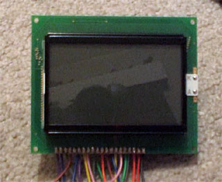
Finally, here's a video of the LCD test in action. It's not very speedy, but will hopefully pick up some speed once I figure out how I'm going to use that Z80180 CPU.
PlayStation Controllers
Monday, 4th February 2008
PlayStation controllers are relatively comfortable, and I have a number of them knocking about.
From top to bottom - PS2 IR remote control and receiver; Guitar Hero wireless Kramer and receiver; black PS2 DualShock 2 analogue joypad; a pair of grey standard PS1 digital joypads.
As I've learned in the past, a decent gamepad can help with certain games. Of course, what's much more fun than playing the games is trying to work out how these controllers work.
The byte-level protocol is very simple; the PlayStation pulls a select line low (used to grab the attention of the controller) then pulses the clock eight times, writing a bit at a time onto one line and reading another bit at a time from another. This means that the controller and PlayStation end up sending and receiving a byte simultaneously. Finally, the PlayStation checks to see if controller pulls the acknowledge line low to indicate that it received the data; if no acknowledgement is received it assumes that there is no controller on the port it is currently accessing.
All electrical connections are unidirectional, and so a controller can be easily connected to a standard PC's parallel port. There are a number of diagrams floating around the internet using similar pin connections, so I followed one of those.
I cut up a pound-shop parallel cable for the PC end and a controller extension cable for the PlayStation end. PlayStation controllers require power; a lot of diagrams I've seen refer to a 9V and 5V supply, some 7.6V and 3.3V. A voltmeter informs me that it's the latter option. Rather than try and draw power from the parallel port, I'm using a generic power supply set to 7.5V. To derive the 3.3V I'm using a 5V regulator followed by two 1A rectifier diodes in series - the diodes provide a voltage drop of 0.7V across each, resulting 3.6V.
I wrote an application in C# that attempted to swap bytes back and forth between the PC and the controller, and was getting good results. I was not, however, having any luck polling the acknowledgement line. It didn't appear to ever go low - my guess was that the program simply couldn't poll the parallel port rapidly enough. Not that this is a slur on C#, of course, but to access the parallel port in the first place I need to use an unmanaged library.
The solution was therefore to write an unmanaged library myself that would handle the PlayStation protocol side of things, which I could then wrap up and add nice functionality to via a C# managed library.
#include "Windows.h"

// inpout32.dll function declarations.
short Inp32(short portAddress);
void Out32(short portAddress, short data);

/// <summary>Gets the state of the data line.</summary>
/// <param name="portAddress">Base address of the parallel port.</param>
/// <returns>The state of the data line.</returns>
extern "C" __declspec(dllexport) bool GetData(short portAddress) {
	return (Inp32(portAddress + 1) & (1 << 6)) != 0;
}

/// <summary>Gets the state of the acknowledge line.</summary>
/// <param name="portAddress">Base address of the parallel port.</param>
/// <returns>The state of the data line.</returns>
extern "C" __declspec(dllexport) bool GetAcknowledge(short portAddress) {
	return (Inp32(portAddress + 1) & (1 << 5)) != 0;
}

/// <summary>Sets the state of the command line.</summary>
/// <param name="portAddress">Base address of the parallel port.</param>
/// <param name="state">The state to set the command line to.</param>
extern "C" __declspec(dllexport) void SetCommand(short portAddress, bool state) {
	Out32(portAddress, (Inp32(portAddress) & ~0x01) | (state ? 0x01 : 0x00));
}

/// <summary>Sets the state of the select line.</summary>
/// <param name="portAddress">Base address of the parallel port.</param>
/// <param name="state">The state to set the select line to.</param>
extern "C" __declspec(dllexport) void SetSelect(short portAddress, bool state) {
	Out32(portAddress, (Inp32(portAddress) & ~0x02) | (state ? 0x02 : 0x00));
}

/// <summary>Sets the state of the clock line.</summary>
/// <param name="portAddress">Base address of the parallel port.</param>
/// <param name="state">The state to set the clock line to.</param>
extern "C" __declspec(dllexport) void SetClock(short portAddress, bool state) {
	Out32(portAddress, (Inp32(portAddress) & ~0x04) | (state ? 0x04 : 0x00));
}

/// <summary>Begins a data transfer by pulling select low.</summary>
/// <param name="portAddress">Base address of the parallel port.</param>
extern "C" __declspec(dllexport) void BeginTransfer(short portAddress) {
	SetSelect(portAddress, false);
}

/// <summary>Ends a data transfer by releasing select high.</summary>
/// <param name="portAddress">Base address of the parallel port.</param>
extern "C" __declspec(dllexport) void EndTransfer(short portAddress) {
	SetSelect(portAddress, true);
}


/// <summary>Exchanges a byte between the PlayStation controller and the PC.</summary>
/// <param name="portAddress">Base address of the parallel port.</param>
/// <param name="data">The data to exchange.</param>
/// <returns>True if the transmission was acknowledged, false if it timed out.</returns>
extern "C" __declspec(dllexport) bool ExchangeByte(short portAddress, unsigned char* data) {

	DWORD TimeoutStart = GetTickCount();

	for (int i = 0; i < 8; ++i) {
		SetClock(portAddress, false);
		SetCommand(portAddress, (*data & (1 << i)) != 0);
		SetClock(portAddress, true);
		if (GetData(portAddress)) {
			*data |= (1 << i);
		} else {
			*data &= ~(1 << i);
		}
	}

	while (GetAcknowledge(portAddress)) {
		if ((GetTickCount() - TimeoutStart) > 10) return false;
	}

	while (!GetAcknowledge(portAddress)) {
		if ((GetTickCount() - TimeoutStart) > 10) return false;
	}

	return true;

}

/// <summary>Exchanges a block of data between the PlayStation controller and the PC.</summary>
/// <param name="portAddress">Base address of the parallel port.</param>
/// <param name="command">The command byte to send.</param>
/// <param name="data">The data to exchange (input and output).</param>
/// <param name="numberOfElements">The size of data in bytes.</param>
/// <returns>The size of the received packet.</returns>
extern "C" __declspec(dllexport) int SendPacket(short portAddress, unsigned char* command, unsigned char* data, int numberOfElements) {

	// Start by sending 0x01.
	unsigned char ToExchange = 0x01;
	if (!ExchangeByte(portAddress, &ToExchange)) return 0;

	// Next send the command byte.
	// Controller will respond with packet size and mode.
	if (!ExchangeByte(portAddress, command)) return 0;

	// Check for end-of-header.
	ToExchange = 0x00;
	if (!ExchangeByte(portAddress, &ToExchange) || ToExchange != 0x5A) return 0;

	// Fix the "numberOfElements" to only try and fetch the number of bytes that are in the packet.
	numberOfElements = min(numberOfElements, (*command & 0xF) * 2);

	for (int i = 0; i < numberOfElements; ++i) {
		if (!ExchangeByte(portAddress, &data[i])) return i + 1;
	}

	return numberOfElements;
}
I'm not much of a C++ programmer, so I hope the above isn't too offensive.
Polling a standard digital joypad or a dual analogue is pretty straightforwards - send 0x42 to the device, and it'll return the status of each button as a bitfield 2 bytes in length. If the controller is in analogue mode, it'll then go on to return a further four bytes; one byte per axis, two axes per joystick.
Standard disclaimer applies; if you're going to hook anything up to your PC, I cannot be held responsible for any damages incurred. Be careful!
I'm still having some problems with data transfer. The controller doesn't always send back enough data (least reliable with a DualShock 2); this could be because I'm running its clock too fast. Introducing delays doesn't seem to help. This is most noticable in the demo program when a DualShock 2 is used in analogue mode; the analogue light flickers on and off.
I also haven't successfully managed to get the DualShock 2 to enter escape mode - this mode is used to access some of the more exotic commands, including commands to control the force feedback motors or to append extra data to the packet sent back when the controller is polled, such as the status of the analogue buttons.
Brass 3 and software PAL
Wednesday, 14th November 2007
My work with the VDP in the Sega Master System made me more aware of how video signals are generated, so thought it would be an interesting exercise to try and generate them in software. This also gives me a chance to test Brass 3, by actively developing experimental programs.
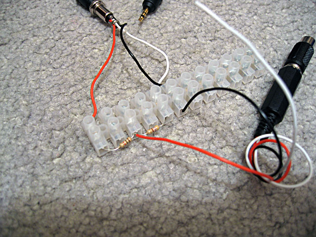
I'm using a simple 2-bit DAC based on a voltage divider, using the values listed here. This way I can generate 0V (sync), ~0.3V (black), ~0.6V (grey) and 1V (white).
My first test was to output a horizontal sync pulse followed by black, grey, then white, counting clock cycles (based on a 6MHz CPU clock). That's 6 clock cycles per µs.

The fastest way to output data to hardware ports on the Z80 is the outi instruction, which loads a value from the address pointed to by hl, increments hl, decrements b and outputs the value to port c. This takes a rather whopping 16 clock cycles (directly outputting to an immediate port address takes 11 clock cycles, but the overhead comes from loading an immediate value into a which takes a further 7). The time spent creating the picture in PAL is 52µs, which is 312 clock cycles. That's 19.5 outi instructions, and by the time you've factored in the loop overhead that gives you a safe 18 pixel horizontal resolution - which is pretty terrible.
Even with this technique, in the best case scenario you output once every 16 clock cycles which gives you a maximum time resolution of 2.67µs. This is indeed a problem as vertical sync is achieved by transmitting two different types of sync pulse, made of either a 2µs sync followed by 30µs black (short) or 30µs sync followed by 2µs black (long). In my case I plumped for the easiest to time 4µs/28µs and hoped it would work.
Anyhow, I made a small three-colour image for testing: ![]() .
.
Of course, as I need to output each scanline anyway I end up with a resolution of 304 lines, which gives me rather irregular pixels, so I just stretch the above image up to 20×304. Eagle-eyed readers would have noticed that the horizontal resolution is only 18 pixels, but somewhere in the development process I forgot how to count and so made the image two pixels too wide.
As you can see, it shows (the entire image is shunted to the right). TVs crop the first and last few scanlines (they aren't wasted, though, and can be used for Teletext) so that's why that's missing. A widescreen monitor doesn't help the already heavily distorted pixels either, but it does (somewhat surprisingly) work.
With a TI-83+ SE (or higher) you have access to a much faster CPU (15MHz) and more accurate timing (crystal timers rather than an RC circuit that changes speed based on battery levels) as well as better interrupt control, so on an SE calculator you could get at least double the horizontal resolution and output correct vertical sync patterns. You also have better control over the timer interrupts, so you could probably drive hsync via a fixed interrupt, leaving you space to insert a game (the only code I had space for checks to see if the On key is held so you can quit the program - more clock cycle counting). I only have the old 6MHz calculator, though, so I'm pleased enough that it works at all, even if the results are useless!
VMusic2 - USB for the 83+
Monday, 21st May 2007
The TI-83+ lacks something the 84+ series has - a USB port.
Enter the VMusic2. This low-cost (£25) module offers a USB host controller with a simple serial interface that can be used to read/write FAT-formatted USB mass storage devices. It can also play MP3 files straight from the drive!
This is all very well, but the TI doesn't have a standard serial port either. To handle communications between the two, therefore, is a PICAXE-28X1 microcontroller.
The TI can then run a program that communicates using its standard linking protocol.
I've posted a thread on MaxCoderz with more information about the project. For those interested in the VMusic2 device, here's a datasheet and here are the commands.
Yes, I know I should probably get a life. I blame the solder fumes.
Parallel-Port SMS Control Pad
Monday, 15th January 2007
I've been wanting to attach an SMS control pad to my PC (and be able to use it to play games with) for a while, so put in an order from those excellent chaps at Rapid for the parts needed.
The joypad (as I've now learned from disassembly) is very primitive - 6 normally-open switches, each connected between a pin on the DE-9 connector and ground. The accepted layout adapter uses the 25-pin parallel port, connecting ground to pin 18, power to pin 1 (not that the control pad uses this pin) and 7 further connections from D0 to D6 for the buttons.
Master System Control Pad and a poorly-soldered DB-25 to DE-9 adapter.
I had been assured that the data lines on parallel ports (D0..D7) were pulled up, and so the layout seemed easy enough - D0..D6 will return highs normally, and when a button is pressed it is connected to ground.
Unfortunately, for whatever reason the data lines on the parallel port on my PC are not pulled up, at least not in any way that I can find to control. However, if you set the lines to be outputs (using bit 5 of the control register), set them all high, then flip them to inputs, they'll read as highs for a while until they float (slowly) back low again. I've used this to my advantage, and so have this:
/// <summary>Flags corresponding to which buttons are pressed.</summary>
[Flags]
public enum Buttons {
    None = 0x00,
    Up = 0x01,
    Down = 0x02,
    Left = 0x04,
    Right = 0x08,
    Button1 = 0x10,
    Button2 = 0x20,
    All = 0x3F,
}

// Retrieve the status of the port.
private Buttons GetRawStatus() {
    // Set D0..D7 as outputs.
    Output(this.BaseAddress + 2, 0x00);
    // Set them high:
    Output(this.BaseAddress + 0, 0xFF);
    // Set D0..D7 as inputs.
    Output(this.BaseAddress + 2, 0x20);
    // Retrieve, invert and mask the data lines.
    return (Buttons)(~(Input(this.BaseAddress + 0)) & (int)Buttons.All);
}
This works very well, with one small problem: nothing is debounced, so pressing any button causes 10 or so press/release actions to be detected until the contacts settle. Therefore, the exposed method for retrieving the status is this:
/// <summary>Gets the status of the buttons from the connected SMS joypad.</summary>
/// <returns>The status of the buttons.</returns>
public Buttons GetStatus() {
    if (!this.Debounced) {
        return GetRawStatus();
    } else {
        Buttons Last = GetRawStatus();
        Buttons Current;
        int MaximumIterations = 100;
        while (((Current = GetRawStatus()) != Last) && (MaximumIterations-- > 0)) {
            Last = Current;
            Thread.Sleep(0);
        }
        return Current;
    }
}
For some strange reason, this doesn't quite work; after a while (or rebooting, or reading/writing the EPP registers) the port starts reading nothing but zeroes again. Running another piece of software that uses the parallel port fixes it.
One missing feature of the emulator was support for the SMS pause button. This button is attached to the Z80's non-maskable interrupt line, so pressing it results in the CPU pushing the program counter to the stack then jumping to $0066.
For most games the pause button just pauses the game, but for some others it will display a menu - such as in Psycho Fox, which lets you use the items you have collected to change animal or use a power-up.

Psycho Fox's in-game menu
One major long-standing bug in the emulator has been interrupt handling by the CPU. I think I've (finally!) got it, though it's still not entirely perfect. How I've set it up now is that a flag is set - IntPending or NmiPending, depending on whether the maskable or non-maskable interrupt pin has been modified - when the interrupt is requested, and cleared when it's been handled.

Japanese Master System BIOS
I have updated the memory emulation to better support BIOS ROMs. Initially, the "Majesco" Game Gear BIOS and some of the "Snail Maze" SMS BIOS worked (though the SMS BIOS would display "Software Error" on several games). I've tested a few of them and they seem to work pretty well.

Hang On and Safari Hunt
Whilst the Japanese BIOS has (in my opinion) the best final effect, it's the M404 prototype BIOS that has the best effect overall:

Internal PS/2 Port
Friday, 6th October 2006
What's that in the bottom left hand corner?
Kerm Martian has added a PS/2 port to his calculator (click the picture for better pictures and the original thread). He has been developing a shell, entitled DoorsCS (click for website) which sports an impressive set of GUI controls - hence the mouse!
Emerson Beta 2
Friday, 22nd September 2006
Sorry about the lack of updates, but I have been incredibly busy with work related programming.
One small project I've had a chance to update is Emerson - my keyboard and mouse library for the TI-83 series calculator.
I know, I can't type layout. Download the library (and demo) here.
TI-83 Plus Mouse
Tuesday, 21st February 2006
I had another go with my AT protocol routines to see if I could persuade a PS/2 mouse to do anything.
It would appear that I could...
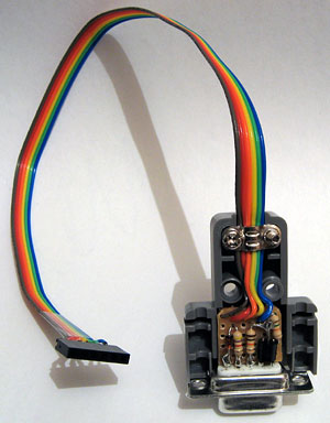
There are two cables for the mouse as there were for the keyboard - one goes to the TI, the other goes to the power supply. The mouse is put into the lowest resolution mode (the cursor is moved 1 pixel per mm).
There's a demo for anyone with a TI-83 Plus and an adapter. It also contains a keyboard demo - and there's a video of that demo here (1MB WMV).
Fortunately, I didn't have to butcher that mouse (it's a rather good miniature USB/PS2 one), but it is connected to the TI with Blu-Tak to keep the wires on the contacts, and isn't very mobile as I only gave the power lead about 15cms clearance. I think it's high time I grabbed myself some proper connectors and a soldering iron from Maplin...
As for the mouse routines - they need a lot of tidying up and making much more reliable, especially in the recovery when a mouse is disconnected then reconnected (my keyboard routines are 'hot pluggable', after all). Extending them to support the Microsoft Intellimouse system, giving the mouse an extra axis (scroll wheel) and two extra buttons would be rather cool as well.
Ultimately, these routines are rather useless until they become widely adopted. Ideally, they could/would be added to a shell, and form part of the standard routines. For example, the shell could provide a "get key" function, which would also transparently return keyboard keys as if they were keys on the keypad, or return four "left" keys if the mouse was moved 4 mm left -- that sort of thing.
Chances of this happening are, sadly, nil.
Subscribe to an RSS feed that only contains items with the Electronics tag.